3D printing and manufacturing method for electronic device with three-dimensional structure

A technology for electronic devices and three-dimensional structures, applied in the direction of multi-layer circuit manufacturing, additive processing, etc., can solve the problems such as the manufacturing requirements of structural electronic devices that cannot meet the function-structural integration, and achieve reduced space occupation and environmental friendliness. Optimum, the effect of improving circuit density

Active Publication Date: 2016-11-16
XI AN JIAOTONG UNIV
View PDF10 Cites 18 Cited by
  • Summary
  • Abstract
  • Description
  • Claims
  • Application Information

AI Technical Summary

Problems solved by technology

It can be seen that the existing process methods cannot meet the manufacturing requirements of structural electronic devices with functional-structural integration, and process innovation is needed to realize the manufacture of new three-dimensional structural electronic devices

Method used


Image

  • 3D printing and manufacturing method for electronic device with three-dimensional structure
  • 3D printing and manufacturing method for electronic device with three-dimensional structure
  • 3D printing and manufacturing method for electronic device with three-dimensional structure

Examples


Embodiment Construction

[0023] The present invention will be further described in detail below in conjunction with the accompanying drawings.

[0024] A 3D printing manufacturing method for a three-dimensional structure electronic device, comprising the following steps:

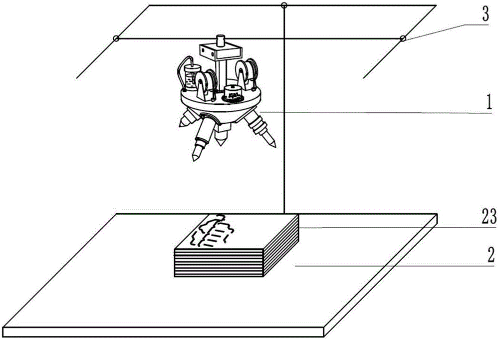
[0025] 1) Refer to figure 1 , according to the performance requirements of the parts to be formed, design the spatial distribution of the circuit in the three-dimensional structure electronic device and the geometric size of the matrix structure, and establish a three-dimensional CAD model; process the model in layers according to the processing direction to obtain the material distribution of each layer section, Write the relative motion program of the print head integrated device 1 and the working platform 2;

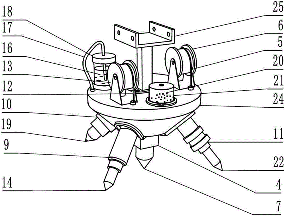
[0026] 2) Select wire printing materials and matrix structure printing materials that meet the performance requirements. Wire printing materials are copper-tin alloys, silver-tin alloys, tin-lead alloys with low melting po...


PUM


Abstract

The invention discloses a 3D printing and manufacturing method for an electronic device with a three-dimensional structure. The 3D printing and manufacturing method comprises the following steps: according to performance requirements of a to-be-formed part, designing spatial distribution of circuits and geometric dimensions of base structures in the electronic device with the three-dimensional structure, establishing a model of three-dimensional CAD, carrying out hierarchical processing on the model according to a processing direction to obtain material distribution of a section at each layer, and writing relative movement programs of a printing head integrated unit and a working platform; then, selecting a conducting wire printing material and a base material printing material which meet the performance requirements; printing a base material, forming the base structures on the working platform; switching the printing head; printing conducting wires; and driving the working platform to descend by a hierarchical thickness by a movement mechanism, repeating a printing process of printing the base material and the conducting wires until all base structures and conducting wires are printed, thereby obtaining the electronic device with the three-dimensional structure. The 3D printing and manufacturing method realizes synchronous printing of conducting wires and a base insulating medium, so that any layout of a three-dimensional space is realized.

Description

technical field [0001] The invention relates to the technical field of structural electronics manufacturing, in particular to a 3D printing manufacturing method of a three-dimensional structural electronic device. Background technique [0002] Structural electronics refers to a three-dimensional electrical structure in which circuits and electronic components are attached or embedded on a substrate structure according to a certain three-dimensional space layout. Its core features are: the electrical part has a three-dimensional spatial layout, which improves the space utilization rate and reduces the volume; the matrix structure has a three-dimensional shape, so that the structural electronics as a whole have certain mechanical properties. Taking advantage of these beneficial properties, structural electronics can be used to manufacture a large number of new electronic devices to realize the integration of function and structure, such as curved surface conformal electronic d...

Claims


Application Information

Patent Timeline
Patent Type & Authority Applications(China)
IPC IPC(8): B22F3/00B22F5/00B29C67/00B33Y10/00H05K3/46B22F10/30B22F10/85B22F12/55
CPCH05K3/46B22F3/00B22F5/00B33Y10/00
Inventor 田小永尹丽仙
Owner XI AN JIAOTONG UNIV
Why Eureka
Try Eureka