Topology structure and wavelength allocation method of staggered-layer 3D optical-on-chip network

An optical on-chip network and topology technology, applied in the architecture with a single central processing unit, the selection device of the multiplexing system, the selection device, etc., can solve the problems of many cross nodes, blocking loss, large loss, etc. The effect of alleviating the blocking of chain building, reducing the blocking probability, and reducing the number of

Active Publication Date: 2019-01-15
XIDIAN UNIV
View PDF3 Cites 0 Cited by
  • Summary
  • Abstract
  • Description
  • Claims
  • Application Information

AI Technical Summary

Problems solved by technology

The routing structure of this 7×7 port router is complex, including at least 36 microring resonators and 8 optical waveguides inside. There are many cross nodes between the optical waveguides and a large number of bent optical waveguides, resulting in large losses
The three-dimensional optical network on chip with 3D-Mesh topology realizes the communication between IP cores of the same layer and IP cores of different layers in the network, but there are problems of serious blocking and loss
However, this wavelength allocation method only alleviates the blocking problem during inter-layer communication, and there is still serious blocking in intra-layer communication.

Method used


Image

  • Topology structure and wavelength allocation method of staggered-layer 3D optical-on-chip network
  • Topology structure and wavelength allocation method of staggered-layer 3D optical-on-chip network
  • Topology structure and wavelength allocation method of staggered-layer 3D optical-on-chip network

Examples


Embodiment Construction

[0031] Below in conjunction with accompanying drawing and embodiment, the present invention is described in further detail:

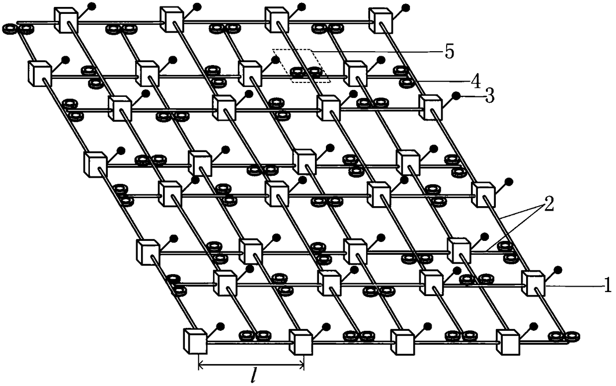
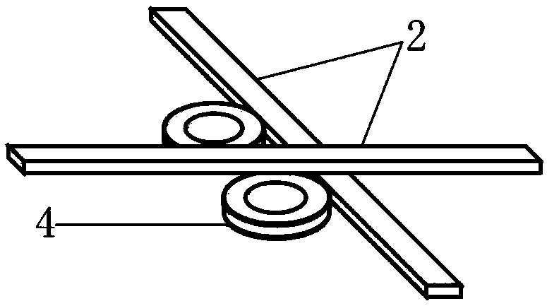
[0032] refer to figure 1 , a topological structure based on a staggered three-dimensional optical network on chip, including upper and lower layers of optical network on chip, each layer of optical network on chip includes a 2D-Mesh topology composed of 4×4 routers 1, where the structure of router 1 Such as figure 2 As shown, adjacent routers 1 are connected through optical waveguides 2, and each router 1 is connected to an IP core 3 through electrical wires. For the relative positional relationship between layers, in the vertical direction, an interlayer micro-ring coupler 4 is built between the upper optical-chip network and the lower optical-chip network; where l represents the distance between adjacent routers 1 in the 2D-Mesh topology. In the optical-on-chip network corresponding to the vacancies of the four single-layer parts at the edge of t...


PUM


Abstract

The invention provides a topological structure based on a staggered three-dimensional light network-on-chip and a wavelength distribution method, and aims to solve the technical problems of serious blockage in the network and high loss in the prior art. The topological structure comprises two layers of 2D-Mesh light networks-on-chip and an interlaminar router; the light networks-on-chip comprise NxN routers connected through optical waveguides; each router is connected with an IP core; the two layers of light networks-on-chip are staggered from each other along the corresponding diagonals, and optical waveguides are added into the light networks-on-chip corresponding to gaps in four single-layer parts on the staggering edges along the optical waveguide directions in the light networks-on-chip; and the interlaminar router is arranged at a position perpendicular to the space where the optical waveguides of the different layer are positioned. The wavelength distribution method of the topological structure comprises the following steps: firstly establishing a three-dimensional coordinate system, and selecting wavelength values; secondly, distributing the wavelength values to all nodes; and finally, configuring a working offset state and temperature of an exchange microring resonator or an interlaminar microring coupler according to the wavelength values distributed to all the nodes.

Description

technical field [0001] The invention belongs to the technical field of on-chip communication, and relates to a topology structure and a wavelength allocation method of a three-dimensional optical on-chip network, in particular to a topological structure and a wavelength allocation method of a three-dimensional optical on-chip network based on a staggered layer, which can be used for network internal cores. reliable communication. Background technique [0002] Network on Chip (Network on Chip, NoC), based on the packet switching method and layered method, realizes the separation of processing units and communication structures: the IP core in the network on chip is connected to the network through routing nodes, and the routers are connected through link nodes. It has good scalability and provides good parallel communication capabilities. The network on chip includes a network on chip using an electrical connection and an optical network on chip (Optical Network on Chip, ONo...

Claims


Application Information

Patent Timeline
Patent Type & Authority Patents(China)
IPC IPC(8): G06F15/173G06F15/78H04Q11/00
CPCG06F15/17387G06F15/7825H04Q11/0062H04Q2011/0052
Inventor 赵介宸顾华玺杨银堂宫怡繁王琨谭伟
Owner XIDIAN UNIV
Why Eureka
Try Eureka