PCB (Printed Circuit Board) chip structure
A chip structure and chip technology, applied in electrical components, electrical solid devices, circuits, etc., can solve the problems of insufficient space for heat sinks, cost increase, insertion, etc., to improve product reliability, simple manufacturing process, and reduce chips. The effect of junction temperature
- Summary
- Abstract
- Description
- Claims
- Application Information
AI Technical Summary
Problems solved by technology
Method used
Image
Examples
Embodiment 1
[0047] Embodiment 1: Making and installing a PCB chip with good heat dissipation function
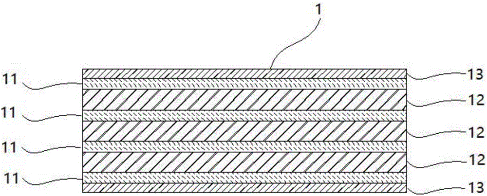
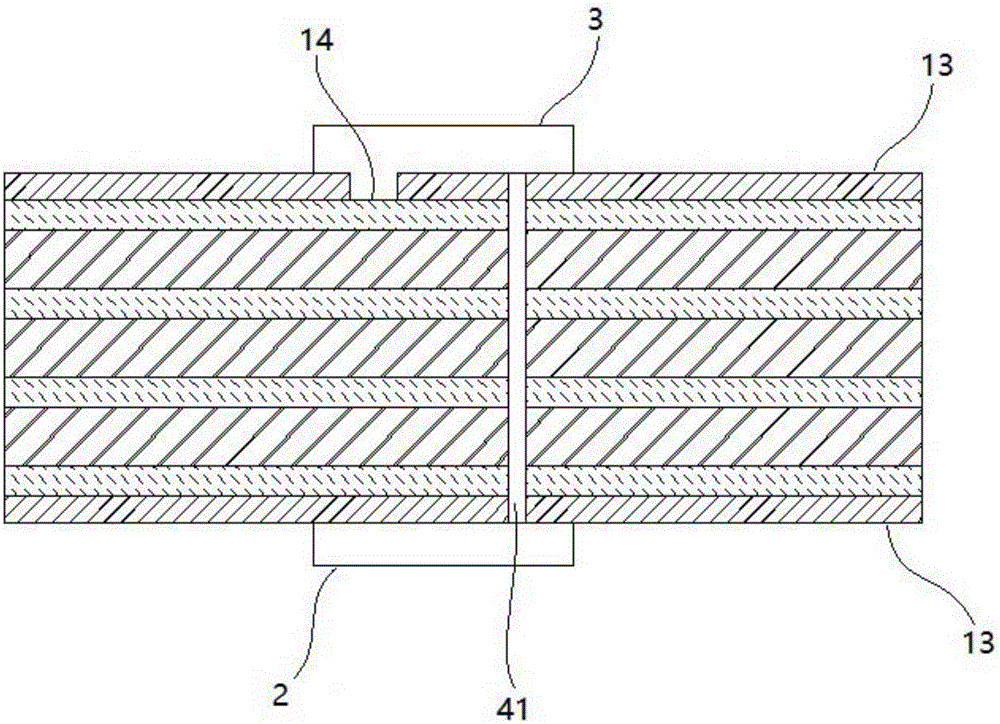
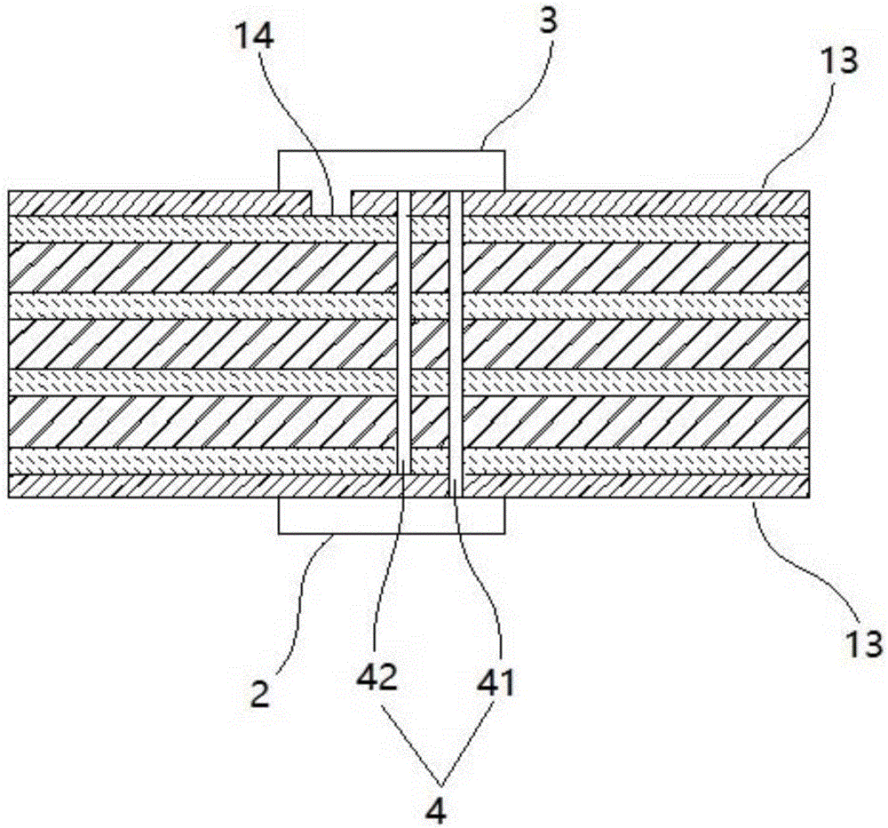
[0048] 101: Make PCB 1: use 4 layers of copper foil 11, and the base material 12 between each adjacent two layers of copper foil 11 (a total of 3 layers of base material 12) are laminated to form a composite layer structure, and the copper foil 11 on the surface of the composite layer The signal line is depicted on the top; a layer of green oil covering layer 13 is covered on the area where the signal line is depicted, and the area where the signal line is not depicted is a copper foil bare area 14, and the copper foil 11 is exposed;
[0049]102: Install chip 2: form a pad corresponding to the pin of chip 2 on one surface of PCB1 through the surface treatment process, and bond the pin of chip 2 to the pad, so that chip 2 is mounted on the surface of PCB1 ;
[0050] 103: Spraying graphite 3: Spray a layer of graphite 3 on the corresponding area of the other side of the PCB1 opposite t...
Embodiment 2
[0052] Embodiment 2: Making and installing a PCB chip with good heat dissipation function
[0053] 201: Make PCB1: use 4 layers of copper foil 11, and the base material 12 between each adjacent two layers of copper foil 11 (a total of 3 layers of base material 12) are laminated to form a composite layer structure, and the outermost copper foil of the composite layer Signal lines are depicted on 11; a layer of green oil covering layer 13 is covered on the area where the signal lines are depicted, and the copper foil bare area 14 is not depicted with signal lines, and the copper foil 11 is exposed;
[0054] 202: Install chip 2: form a pad corresponding to the pin of chip 2 on one surface of PCB1 through the surface treatment process, and bond the pin of chip 2 to the pad, so that chip 2 is mounted on the surface of PCB1 ;
[0055] 203: Spraying graphite 3: using carbon technology, spray a layer of graphite 3 on the corresponding area on the other side of PCB1 opposite to the ab...
PUM
 Abstract
Description
Claims
Application Information


