How to make a flat vdmos

A manufacturing method and planar technology, which is applied in semiconductor/solid-state device manufacturing, electrical components, circuits, etc., can solve the problems of high manufacturing cost and long manufacturing cycle, and achieve the goal of reducing manufacturing cost, heat treatment process, and shortening the manufacturing cycle Effect

Active Publication Date: 2019-02-12
FOUNDER MICROELECTRONICS INT
View PDF3 Cites 0 Cited by
  • Summary
  • Abstract
  • Description
  • Claims
  • Application Information

AI Technical Summary

Problems solved by technology

[0013] The invention provides a method for manufacturing planar VDMOS, which is used to solve the problems of high production cost and long production cycle in the prior art

Method used


Image

  • How to make a flat vdmos
  • How to make a flat vdmos
  • How to make a flat vdmos

Examples


Embodiment 1

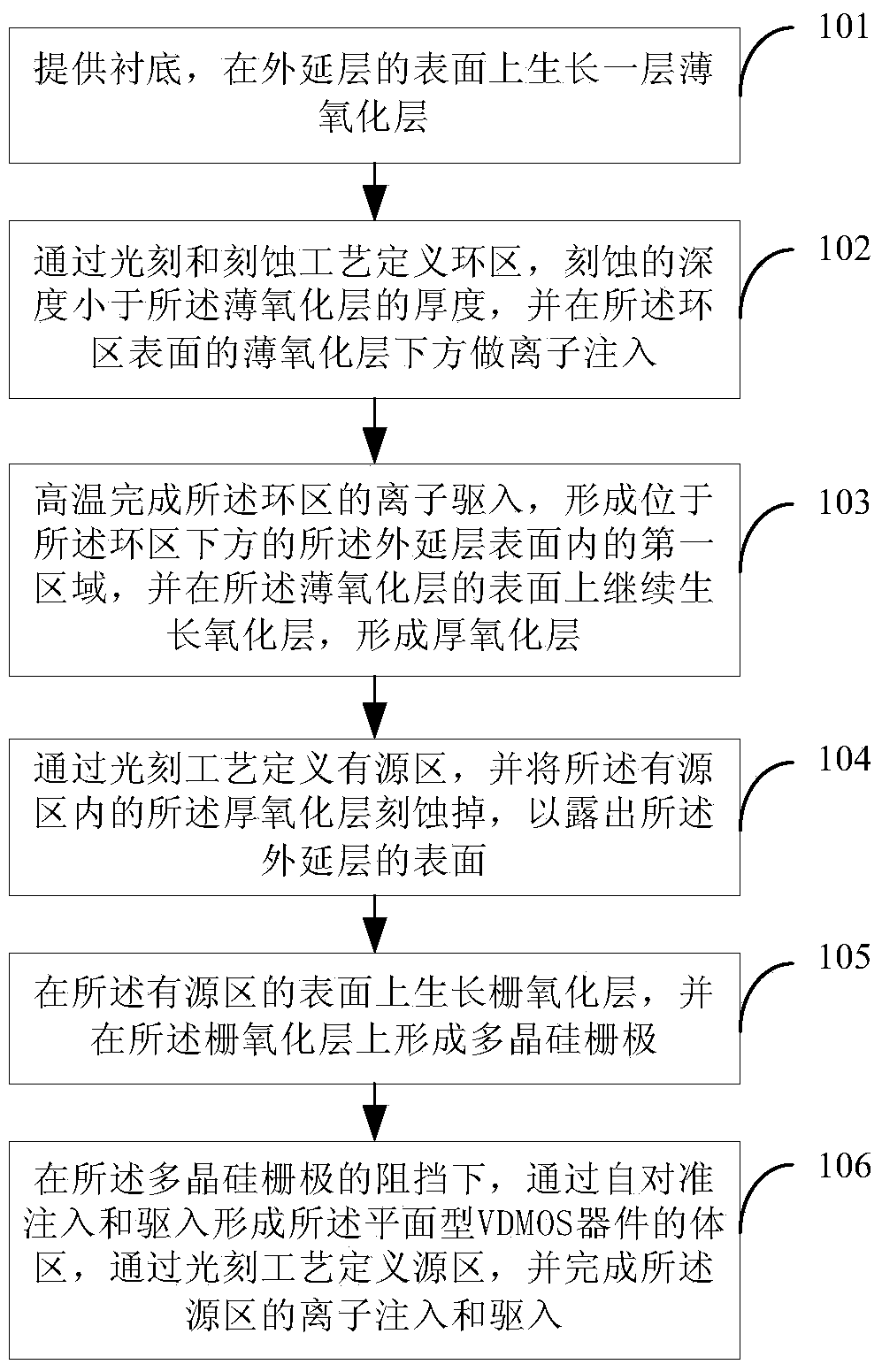
[0032] figure 1 A schematic flow chart of the planar VDMOS manufacturing method provided in Embodiment 1 of the present invention, as shown in figure 1 As shown, the planar VDMOS manufacturing method provided in this embodiment includes the following steps:

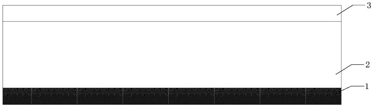
[0033] Step 101, providing a substrate, and growing a thin oxide layer on the surface of the epitaxial layer;

[0034] specific, figure 2 It is a schematic structural diagram of the planar VDMOS after performing step 101, as figure 2 As shown, preferably, the substrate provided in this embodiment includes an N-type substrate 1 and an N-type epitaxial layer 2 . The substrate is thermally oxidized for 30-60 minutes at a temperature of 900-1100 degrees to form a thin oxide layer 3 with a thickness of 1000-2000 angstroms.

[0035] Step 102, define the ring area by photolithography and etching process, the etching depth is less than the thickness of the thin oxide layer, and perform ion implantation under the thin oxide ...

Embodiment 2

[0049] Figure 7 A schematic flow chart of the planar VDMOS fabrication method provided in Embodiment 2 of the present invention, as shown in Figure 7 As shown, the planar VDMOS manufacturing method provided in this embodiment includes:

[0050] Step 201, providing a substrate, and growing a thin oxide layer on the surface of the epitaxial layer;

[0051] Step 202, define the ring area by photolithography and etching process, the etching depth is less than the thickness of the thin oxide layer, and perform ion implantation under the thin oxide layer on the surface of the ring area;

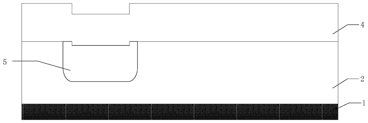
[0052] Step 203, complete the ion drive into the ring region at high temperature to form a first region on the surface of the epitaxial layer below the ring region, and continue to grow an oxide layer on the surface of the thin oxide layer to form a thick oxide layer;

[0053] Step 204, define an active region by a photolithography process, and etch away the thick oxide layer in the active reg...


PUM


Abstract

The invention provides a planar VDMOS manufacturing method. The planar VDMOS manufacturing method comprises the steps of: growing a thin oxidation layer on the surface of an epitaxial layer; defining a loop region through photoetching and etching processes, and carrying out ion implantation under the thin oxidation layer on the surface of the loop region, wherein the etching depth is less than the thickness of the thin oxidation layer; carrying out ion drive-in in the loop region to form a first region in the surface of the epitaxial layer under the loop region, and growing an oxidation layer on the surface of the thin oxidation layer continuously to form a thick oxidation layer; defining an active region, and etching out the thick oxidation layer in the active region; growing a gate oxidation layer on the surface of the active region, and forming polysilicon gates on the gate oxidation layer; and forming a body region through self-aligned implantation and drive-in, defining source regions, and completing ion implantation and drive-in, wherein the body region surrounds the source regions, partial regions of the body region and the source regions extend below the polysilicon gates, and the depth of the body region is less than that of the first region. The planar VDMOS manufacturing method only needs two long-time high-temperature heat treatment processes, reduces cost and shortens manufacturing period.

Description

technical field [0001] The invention relates to the field of semiconductor chip manufacturing, in particular to a method for manufacturing planar VDMOS. Background technique [0002] Vertical double-diffused field-effect transistor (VDMOS) is one of the most commonly used power transistors at present. As a voltage-controlled device, the gate voltage signal controls the formation of the channel, thereby controlling the conduction of the source and drain currents. VDMOS has the advantages of both bipolar transistors and ordinary MOS devices, and is widely used in the field of switching power supplies. [0003] The traditional planar VDMOS fabrication method is as follows: [0004] Step 1. Initially oxidize a thick oxide layer on the epitaxial layer. The thickness of the thick oxide layer is generally greater than 10,000 angstroms, the oxidation temperature is between 1050-1200 degrees, and the oxidation time is between 250-400 minutes; [0005] Step 2, define the ring area b...

Claims


Application Information

Patent Timeline
Patent Type & Authority Patents(China)
IPC IPC(8): H01L21/336
Inventor 闻正锋邱海亮马万里赵文魁
Owner FOUNDER MICROELECTRONICS INT
Why Eureka
Try Eureka