Edge-trimmed composite back sealing layer structure used for silicon wafer, and manufacturing method thereof
A manufacturing method and layer structure technology, applied in semiconductor/solid-state device manufacturing, semiconductor/solid-state device components, semiconductor devices, etc., can solve problems such as pyramids, edge stacking faults, and particle pollution
- Summary
- Abstract
- Description
- Claims
- Application Information
AI Technical Summary
Problems solved by technology
Method used
Image
Examples
Embodiment Construction
[0017] The composite back-sealing layer structure with edge removal and its manufacturing method for silicon wafers according to the present invention will be further described in detail in conjunction with the accompanying drawings.
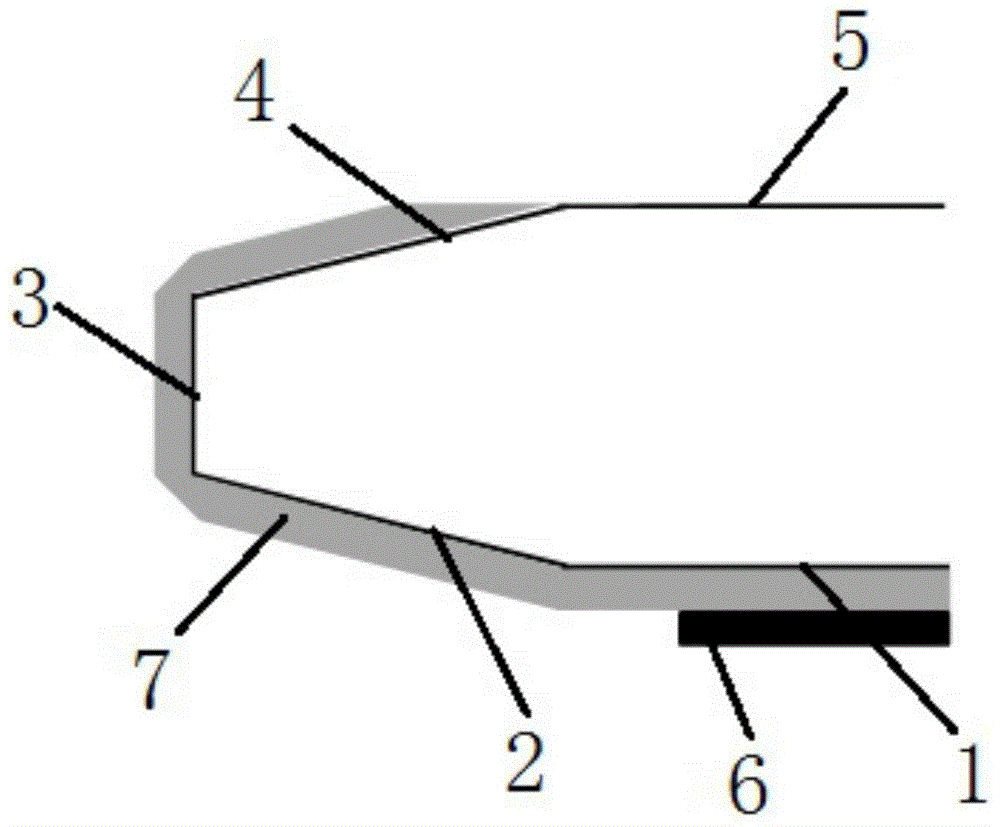
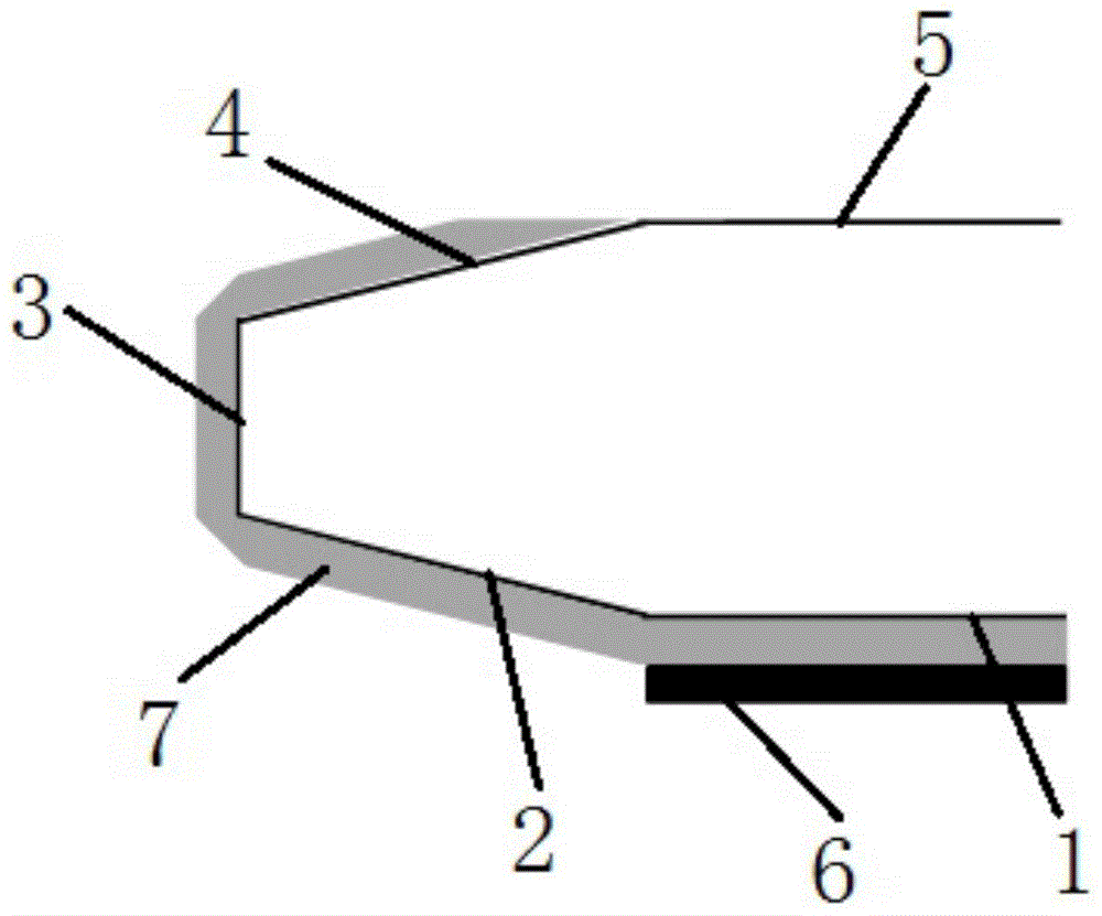
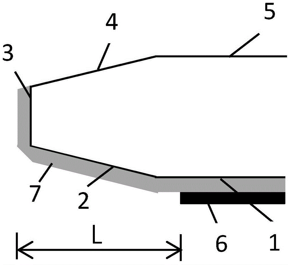
[0018] Such as image 3 , Figure 4 As shown, the compound back-sealing layer structure with edge removal used in the present invention for silicon wafers completely covers the polysilicon back-sealing layer 7 on the back side 1, back bevel region 2, and edge region 3 of the silicon wafer. The outer side of the polysilicon back-sealing layer 7 on the back side 1 of the silicon wafer is covered with a silicon dioxide back-sealing layer 6 . The front side 5 of the silicon wafer is the polishing surface. The bevel region 4 on the front side of the silicon wafer is a smooth monocrystalline silicon surface without polycrystalline silicon film coverage. The polysilicon back-sealing layer 7 covers the back side 1, the back bevel area 2 and the edge ...
PUM
 Abstract
Description
Claims
Application Information


