De-edged super back seal layer structure for silicon wafer and manufacturing method thereof

A layer structure, silicon wafer technology, applied in semiconductor/solid-state device manufacturing, semiconductor/solid-state device components, semiconductor devices, etc., can solve problems such as pyramids, particle pollution, edge stacking faults, etc.

Active Publication Date: 2016-11-23
上海中欣晶圆半导体科技有限公司
View PDF5 Cites 7 Cited by
  • Summary
  • Abstract
  • Description
  • Claims
  • Application Information

AI Technical Summary

Problems solved by technology

[0005] The object of the present invention is to provide a super back-sealing layer structure with edge removal for silicon wafers a...

Method used


Image

  • De-edged super back seal layer structure for silicon wafer and manufacturing method thereof
  • De-edged super back seal layer structure for silicon wafer and manufacturing method thereof
  • De-edged super back seal layer structure for silicon wafer and manufacturing method thereof

Examples


Embodiment Construction

[0018] The structure of the super back-sealing layer with edge removal and its manufacturing method for silicon wafers according to the present invention will be further described in detail below in conjunction with the accompanying drawings.

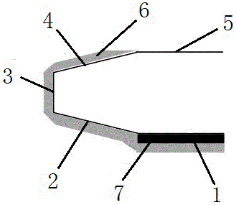
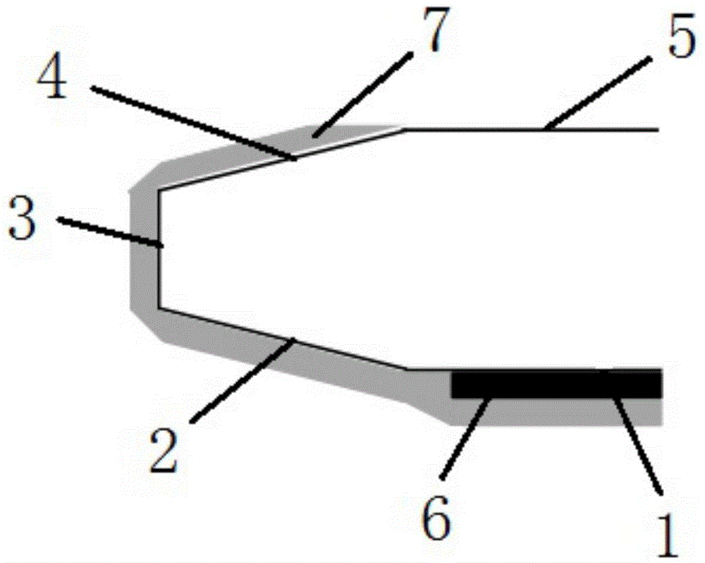
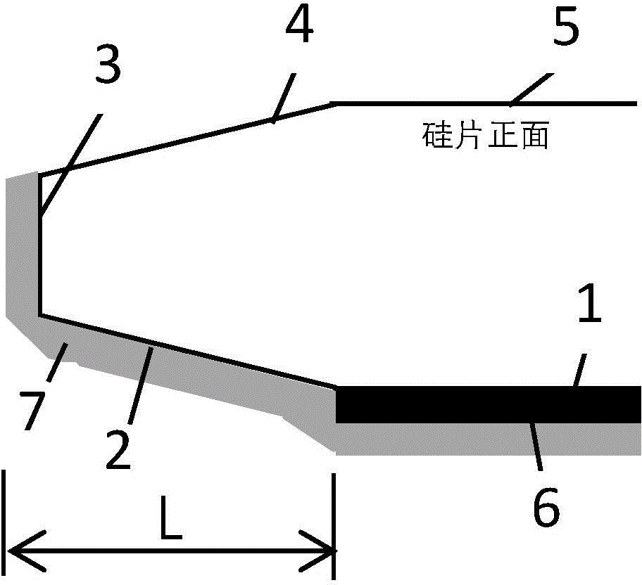
[0019] Such as image 3 , Figure 4 As shown, the present invention is used for silicon wafers with a super back-sealing layer structure with edge removal. The back-sealing layer is completely covered on the back side 1, the back bevel area 2, and the edge area 3 of the silicon wafer, so as to maximize the back-sealing effect. The front side 5 of the silicon wafer is the polishing surface. The bevel region 4 on the front side of the silicon wafer is a smooth monocrystalline silicon surface without polycrystalline silicon film coverage. The silicon dioxide back-sealing layer 6 covers the back side 1 of the silicon wafer, and the polysilicon back-sealing layer 7 covers the outer side of the silicon dioxide back-sealing layer 6 , coveri...


PUM

PropertyMeasurementUnit
Thicknessaaaaaaaaaa
Thicknessaaaaaaaaaa

Abstract

The invention provides a de-edged super back seal layer structure for a silicon wafer. The structure comprises a silicon dioxide back seal layer, wherein the silicon dioxide back seal layer is covered on the back surface of the silicon wafer; and a polycrystalline silicon back seal layer, wherein the polycrystalline silicon back seal layer is covered on the outer side of the silicon dioxide back seal layer and covers the back surface of the silicon wafer, a back surface slope edge area and an edge area. According to the de-edged super back seal layer structure for the silicon wafer, the positive surface slope edge of the silicon wafer only has monocrystalline silicon serving as a body material, and has a high-quality smooth surface, which hardly has no difference with a polished surface. The monocrystalline silicon layer is grown on the positive surface slope edge and the polished surface of the silicon wafer during epitaxy, so that seamless connection can be realized, stratification phenomenon does not occur, the problems of particle pollution, edge dislocation and pyramid in epitaxy are also solved, and process yield rate is improved.

Description

technical field [0001] The invention relates to the fields of semiconductors and material production applications, in particular to a super back-seal layer structure with edge-cutting for silicon wafers and a manufacturing method thereof. Background technique [0002] The back seal design of the silicon wafer has an important impact on the subsequent epitaxial process. Improper back seal design will cause problems such as self-doping and abnormal growth of silicon slag on the back, resulting in the loss of the yield of the epitaxial process. [0003] Super back seal is a kind of back seal technology developed in recent years. figure 1 with figure 2 Shown is a common silicon wafer super back seal design with edge removal treatment, the inner layer is a silicon dioxide back seal layer, and the outer layer is a polysilicon back seal layer. This design has a more obvious effect on solving the problems of self-doping and abnormal growth of silicon slag on the back surface duri...

Claims


Application Information

Patent Timeline
IPC IPC(8): H01L23/29H01L23/31H01L21/02
Inventor 千津井勝己贺贤汉洪漪
Owner 上海中欣晶圆半导体科技有限公司
Why Eureka
Try Eureka