A self-aligned dual pattern imaging method
A technology of double patterning and imaging method, which is applied in the photoplate making process of pattern surface, microlithography exposure equipment, instruments, etc., can solve the problems of self-aligned double pattern imaging, such as time-consuming, high cost, and large consumption of raw materials. , to achieve the effect of reducing the steps of coating photoresist, reducing the flow and reducing the cost
- Summary
- Abstract
- Description
- Claims
- Application Information
AI Technical Summary
Problems solved by technology
Method used
Image

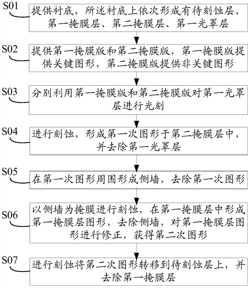

Examples
Embodiment 1
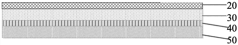
[0045] Step S01, providing a substrate (not shown in the figure), on which the layer to be etched 50, the first mask layer 40, the second mask layer 30, and the first mask layer 20 are sequentially formed, such as image 3 shown.
[0046]In this embodiment, a substrate to be processed is provided, and the substrate may be a Si substrate, a Ge substrate, a SiGe substrate, an SOI (Silicon On Insulator, silicon on insulator) substrate, or the like. In other embodiments, it can also be a substrate including other elemental semiconductors or compound semiconductors, such as GaAs, InP or SiC, etc., it can also be a stacked structure, such as Si / SiGe, etc., and it can also be other epitaxial structures, such as SGOI (Silicon germanium on insulator) and so on. In this embodiment, the substrate is a bulk silicon substrate, and a layer to be etched 50, a first mask layer 40, a second mask layer 30, and a first mask layer 20 are formed on the substrate. Refer to figure 2 shown.
[00...
Embodiment 2
[0076] In this embodiment, different from Embodiment 1, the photolithography process in this embodiment is completed by using negative photoresist and positive developing process, and at the same time, the method of correcting the photoresist is adopted to finally achieve the first mask The layer graph 400 is corrected to obtain the second graph 410 . In this embodiment, only the different parts from the first embodiment are described, and the same parts are only briefly explained.
[0077] Step S11, providing a substrate on which the layer to be etched 50, the first mask layer 40, the second mask layer 30, and the first mask layer 20 are sequentially formed, such as image 3 shown.
[0078] In this embodiment, the substrate is a Ge substrate, which is mainly used in the field of high-speed devices. And a layer to be etched 50 , a first mask layer 40 , a second mask layer 30 , and a first mask layer 20 are formed on the substrate. The layer to be etched 50 , the first mask ...
PUM
 Abstract
Description
Claims
Application Information
 - R&D
- Intellectual Property
- Life Sciences
- Materials
- Tech Scout
- Unparalleled Data Quality
- Higher Quality Content
- 60% Fewer Hallucinations
Browse by: Latest US Patents, China's latest patents, Technical Efficacy Thesaurus, Application Domain, Technology Topic, Popular Technical Reports.
© 2025 PatSnap. All rights reserved.Legal|Privacy policy|Modern Slavery Act Transparency Statement|Sitemap|About US| Contact US: help@patsnap.com