Semiconductor structure and forming method thereof

A technology of semiconductor and dry etching, applied in the direction of semiconductor devices, semiconductor/solid-state device manufacturing, electrical components, etc., can solve problems such as sidewall 33 damage, uneven mask layer thickness, and affect the quality of fins, so as to avoid The effect of excessive thickness

Active Publication Date: 2016-12-07
SEMICON MFG INT (SHANGHAI) CORP
View PDF3 Cites 15 Cited by
  • Summary
  • Abstract
  • Description
  • Claims
  • Application Information

AI Technical Summary

Problems solved by technology

[0011] Figure 5 It is a schematic diagram of the structure in an ideal state after removing the sacrificial layer 31 in the prior art, but in an actual process, removing the sacrificial layer 31 will often cause damage to the sidewall 33 or damage to the oxide layer 20, resulting in the underside of the sidewall 33. The thickness of the mask layer is not uniform (please refer to Image 6 ), affecting the quality of the final formed fin
Therefore, the performance of the semiconductor structure formed by the prior art still needs to be further improved.

Method used


Image

  • Semiconductor structure and forming method thereof
  • Semiconductor structure and forming method thereof
  • Semiconductor structure and forming method thereof

Examples


Embodiment Construction

[0043] As mentioned in the background art, the performance of the semiconductor structure formed in the prior art still needs to be further improved.

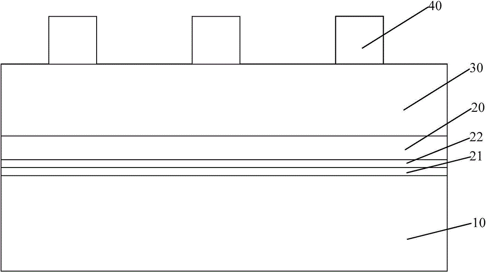
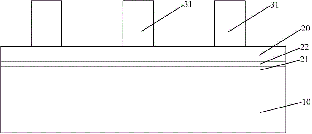
[0044] Research has found that in the actual process, the sacrificial layer 31 (please refer to Figure 4 ) is generally made of materials that are easier to remove such as amorphous carbon or polysilicon layer. When the material of the sacrificial layer 31 is amorphous carbon, the etching selectivity of the amorphous carbon and silicon oxide is relatively low, and in the process of removing the sacrificial layer 31, it is easy to cause damage to the silicon oxide layer 20 (please refer to Image 6 ), so that the thickness of the mask layer is not uniform.

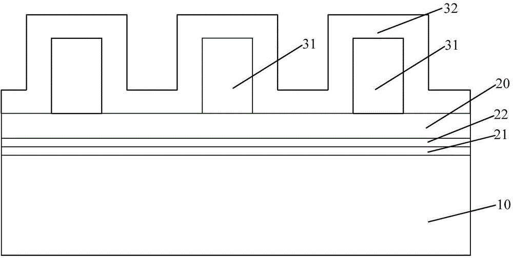
[0045] Please refer to Figure 7 , using the sidewall 33 as a mask to etch the mask layer and the semiconductor substrate 10 to form the fin portion 11 . Due to the non-uniform thickness of the mask layer, the finally formed fins 11 have non-uniform heights. Thus affec...


PUM


Abstract

The invention provides a semiconductor structure and a forming method thereof. The forming method of the semiconductor structure comprises the steps that a semiconductor substrate is provided; a mask layer and a sacrificial material layer located on the surface of the mask layer are sequentially formed on the surface of the semiconductor substrate; the sacrificial material layer is etched to form a plurality of discrete sacrificial layers; side walls are formed on the side wall surfaces of the sacrificial layers; the sacrificial layers are removed; and supplement side walls are formed on the side wall surfaces of the side walls. By the method, improvement of the performance of the formed semiconductor structure is facilitated.

Description

technical field [0001] The invention relates to the technical field of semiconductors, in particular to a semiconductor structure and a forming method thereof. Background technique [0002] With the continuous development of semiconductor process technology, the process node is gradually reduced, and the gate-last (gate-last) process has been widely used to obtain an ideal threshold voltage and improve device performance. However, when the feature size (CD, Critical Dimension) of the device is further reduced, even if the gate-last process is adopted, the structure of the conventional MOS field effect transistor can no longer meet the requirements for device performance, and the fin field effect transistor (Fin FET) as Substitution of conventional devices has received extensive attention. [0003] As the minimum line width and spacing of integrated circuit designs continue to shrink, fin field effect transistor (FinFET) fin widths are getting smaller and smaller. When the ...

Claims


Application Information

Patent Timeline
Patent Type & Authority Applications(China)
IPC IPC(8): H01L21/336H01L29/78
Inventor 张海洋肖芳元
Owner SEMICON MFG INT (SHANGHAI) CORP
Why Eureka
Try Eureka