Low-power-consumption scanning testing method and device based on parallel applying of test excitation

A technology of test excitation and scan test, which is applied in the direction of measuring devices, electronic circuit testing, and measuring electronics, can solve the problems of large dynamic power consumption of combinational logic, large shift power consumption of scanning units, and large power consumption of clock trees, etc., to achieve Effects of reduced power consumption, reduced dynamic power consumption, and reduced peak power consumption

Active Publication Date: 2016-12-14
NAT UNIV OF DEFENSE TECH
View PDF5 Cites 2 Cited by
  • Summary
  • Abstract
  • Description
  • Claims
  • Application Information

AI Technical Summary

Problems solved by technology

[0009] 1. The huge shift power consumption of the scan unit in the serial shift mode: due to the above-mentioned testability design of the traditional multi-scan chain structure, a large number of serial shift operations will be performed in the scan test mode, but any test stimulus (or Test response) in 0 → 1 or 1 → 0 jump, will be passed along each scan unit on the scan chain until the group of test stimuli is applied (or the capture response of the previous group of stimuli is completely removed);
[0010] 2. Huge dynamic power consumption of combinatorial logic in serial shift mode: due to the frequent flipping of the value of the scan unit (take the scan flip-flop as an example) in the testability design of the above-mentioned traditional multi-scan chain structure, the scan flip-flop The combinational logic driven by the Q terminal will also jump due to the jump of the Q terminal value, thereby generating unnecessary combinational logic flipping power consumption
[0011] 3. The huge power consumption of the clock tree during the test: by figure 2 It can be seen that during the entire test process, the test clock of each scan chain is active. For large-scale chip design, the power consumption of the clock tree will account for a large part

Method used


Image

  • Low-power-consumption scanning testing method and device based on parallel applying of test excitation
  • Low-power-consumption scanning testing method and device based on parallel applying of test excitation
  • Low-power-consumption scanning testing method and device based on parallel applying of test excitation

Examples


Embodiment 1

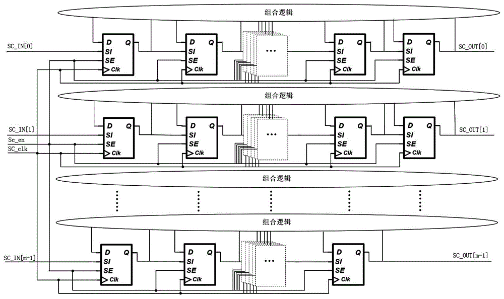
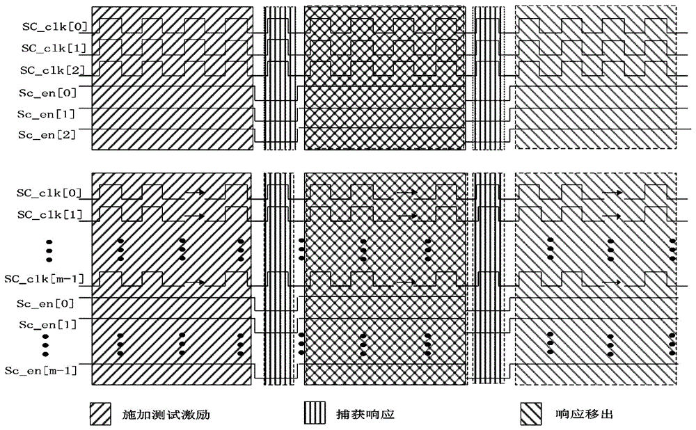
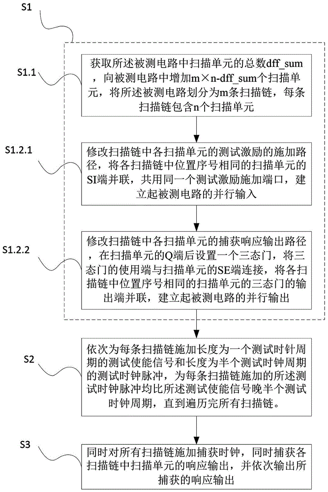
[0054] Such as image 3 As shown, the present embodiment 1. A low-power scanning test method based on parallel application of test excitations includes the following steps: S1. dividing and constructing scanning units in the circuit under test into several equal-length scan chains; S2. Apply test enable signals and test clock pulses to each scan chain in turn until all scan chains have been traversed; S3. Simultaneously apply capture clocks to all scan chains, capture the response output of the scan units in each scan chain at the same time, and output the captured response output. In this draft example, the specific steps of step S1 are: S1.1. Obtain the total number dff_sum of scanning units in the circuit under test, add m×n-dff_sum virtual scanning units to the circuit under test, and divide the circuit under test into There are m scan chains, each scan chain includes n scan units; S1.2. Interrupt the serial path between each scan unit in the scan chain, and establish par...


PUM


Abstract

The invention discloses a low-power-consumption scanning testing method and device based on the parallel applying of test excitation, and the method comprises the steps: S1, enabling a scanning unit in a tested circuit to be divided and built into a plurality of scanning links with equal lengths; S2, sequentially applying a testing enabling signal and testing clock pulse to each scanning link till the traversal of all scanning links is completed; S3, applying a capturing clock to all links at the same time, capturing the response output of the scanning units in all scanning links at the same time, and sequentially outputting the captured response output. The low-power-consumption scanning testing implements the method. The device comprises a scanning link building module, a scanning excitation module and a scanning capturing module. The method is simple in implementation, is high in flexibility, is low in power consumption, is short in testing time, and can be suitable for the scanning testing of a plurality of scanning links.

Description

technical field [0001] The invention relates to the technical field of scan test of integrated circuits, in particular to a low power consumption scan test method and device. Background technique [0002] With the further reduction of the size of the integrated circuit process, the manufacturing yield is becoming more and more difficult to guarantee, and the design for test has become an increasingly indispensable technology for the development and manufacture of today's chips. However, because the fault test emphasizes high fault coverage and short test time, the flip probability of the internal logic of the chip caused by the stimulus of the fault test is much greater than that of the internal logic of the chip in the normal function mode, resulting in several times the power consumption of the test power consumption in normal functional mode. If the chip is in a state of high power consumption for a long time during the test process, or if the peak power consumption exce...

Claims


Application Information

Patent Timeline
Patent Type & Authority Applications(China)
IPC IPC(8): G01R31/28
CPCG01R31/2851
Inventor 郭阳邓丁宋结兵李振涛张臻阳
Owner NAT UNIV OF DEFENSE TECH
Why Eureka
Try Eureka