Fluorescence waveguide light condensation module, solar power generation device and application thereof
A fluorescent and waveguide technology, applied in the field of solar power generation, can solve the problem of low utilization rate of sunlight, achieve the effect of isolating ultraviolet rays, excellent heat insulation and sound insulation, and improving utilization
- Summary
- Abstract
- Description
- Claims
- Application Information
AI Technical Summary
Problems solved by technology
Method used
Image

Examples
no. 1 Embodiment
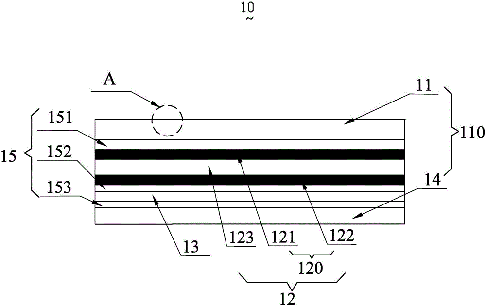
[0044] The layer structure of the fluorescent waveguide concentrating module 10 along the sunlight incident direction is as follows:
[0045] The first glass waveguide layer 11-the first dielectric layer 151-the first fluorescent layer 121-the optical thinning dielectric layer 123-the second fluorescent layer 122-the second dielectric layer 152-the reflective layer 13-the third dielectric layer 153-the The second glass waveguide layer 14 is described.
[0046] Wherein, the material of the first glass waveguide layer 11 and the second glass waveguide layer 14 is tempered glass, and its thickness is 4 mm;
[0047] The materials of the first dielectric layer 151, the second dielectric layer 152 and the third dielectric layer 153 are respectively ITO, and the thicknesses of the three are all 100 nm;
[0048] The material of the first fluorescent layer 121 is a ZnO thin film material with a thickness of 3 μm; the material of the second fluorescent layer 122 is a CdS thin film mate...
no. 2 Embodiment
[0052] The difference between the second specific embodiment and the first specific embodiment is that: the thickness of the first fluorescent layer 121 is 10 μm; the thickness of the second fluorescent layer 122 is 1 μm.
[0053] Through the same test method as that of the above-mentioned first specific embodiment, it is obtained that the utilization rate of sunlight of the fluorescent waveguide concentrating module 10 can reach 95%.
no. 3 Embodiment
[0055] The difference between the third specific embodiment and the first specific embodiment is that: the thickness of the first fluorescent layer 121 is 1.3 μm; the thickness of the second fluorescent layer 122 is 9.7 μm.
[0056] Through the same test method as that of the above-mentioned first specific embodiment, it is obtained that the utilization rate of sunlight of the fluorescent waveguide concentrating module 10 can reach 90%.
[0057] In this embodiment, the materials and thicknesses selected for each layer in the fluorescent waveguide concentrating module 10 will affect the utilization rate of sunlight by the fluorescent waveguide concentrating module 10, that is, the transmittance of visible light. The above-mentioned specific embodiments in the present invention are only examples, and are not intended to limit the present invention.
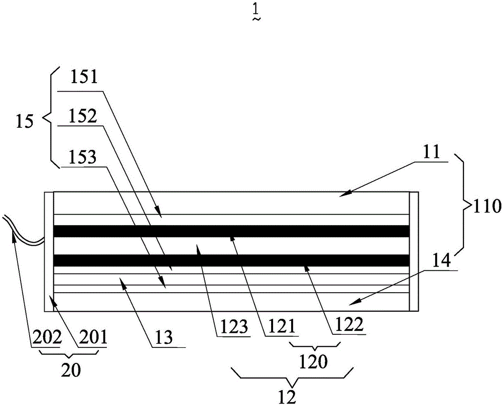
[0058] see image 3 The second embodiment of the present invention provides a solar power generation device 1 for converting sunl...
PUM
| Property | Measurement | Unit |
|---|---|---|
| Thickness | aaaaa | aaaaa |
| Thickness | aaaaa | aaaaa |
| Thickness | aaaaa | aaaaa |
Abstract
Description
Claims
Application Information