A kind of qled device based on metal/metal oxide and preparation method thereof

A technology based on oxides and metals, applied in the field of metal/metal oxide-based QLED devices and their preparation, can solve the problems of high hole injection barriers of QLED devices, achieve the effects of reducing defect states, reducing potential barriers, and improving performance

Active Publication Date: 2019-12-10
TCL CORPORATION
View PDF6 Cites 0 Cited by
  • Summary
  • Abstract
  • Description
  • Claims
  • Application Information

AI Technical Summary

Problems solved by technology

[0004] In view of the above-mentioned deficiencies in the prior art, the object of the present invention is to provide a metal / metal oxide-based QLED device and its preparation method, aiming to solve the problem of high hole injection barrier of existing QLED devices

Method used


Image

  • A kind of qled device based on metal/metal oxide and preparation method thereof
  • A kind of qled device based on metal/metal oxide and preparation method thereof
  • A kind of qled device based on metal/metal oxide and preparation method thereof

Examples


Embodiment 1

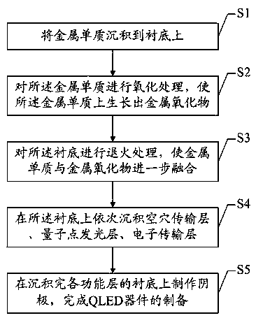
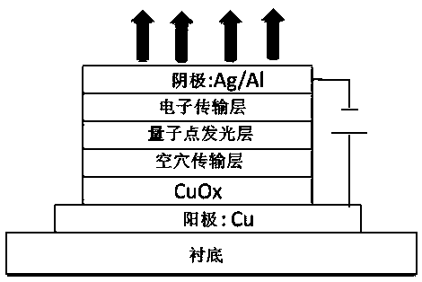
[0044] Embodiment one uses Cu / CuO x Fabrication of QLED devices with the structure as the bottom electrode

[0045] 1), using the method of steaming to deposit metal elemental Cu on the substrate, its thickness is 200nm;

[0046] 2), put the substrate part deposited with metal elemental Cu into hydrogen peroxide (use hydrogen peroxide with a volume ratio of 30%, wherein a small amount of acetic acid is added, and the volume ratio of acetic acid to the total solution is 0.02-0.1%), and the metal elemental Cu is Oxidation for 2h to control the thickness of copper oxide, making CuO x directly grown on metallic Cu. Or heating the substrate deposited with metal element Cu in oxygen to oxidize metal element Cu, the heating temperature is 300°C, and the reaction time is 1h;

[0047] 3), the substrate is annealed at a temperature of 200°C in nitrogen, and the annealing time is 20min, so that Cu and CuO x Further effect, one is to make copper oxide can be reduced in a small amount ...

Embodiment 2

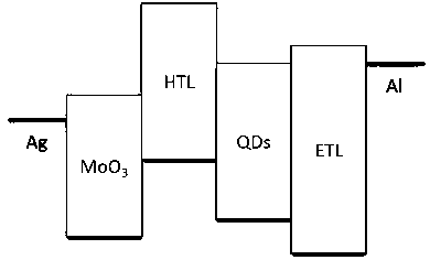
[0052] Embodiment 2 uses Mo / MoO x Fabrication of QLED devices with the structure as the bottom electrode

[0053] 1), Mo is deposited on the substrate by the method for magnetron sputtering, and its thickness is between 150nm;

[0054] 2), then put the substrate part deposited with metal elemental Mo into hydrogen peroxide (use 30% hydrogen peroxide by volume, wherein a small amount of acetic acid is added, and acetic acid accounts for 0.02-0.1% by volume of the total solution) to oxidize the metal elemental Mo 1h, to control the thickness of molybdenum oxide, so that copper oxide grows directly on the metal elemental Cu. Or oxidize the metal elemental Mo by heating it in oxygen, the heating temperature is 250°C, and the reaction time is 1h;

[0055] 3) Anneal the substrate grown on molybdenum oxide at 250°C in nitrogen, and the annealing time is 15min, which can make Mo and MoO x Further function, one is to make molybdenum oxide a small amount of reduction to generate oxyg...


PUM

PropertyMeasurementUnit
electron work functionaaaaaaaaaa

Abstract

The invention discloses a metal / metal oxide-based QLED device and a preparation method thereof. The preparation method includes: step A, depositing a simple metal substance on a substrate; step B, performing oxidation treatment on the simple metal substance, so that a metal oxide grows on the simple metal substance; step C, annealing the substrate treatment to further fuse the metal element with the metal oxide; step D, sequentially depositing a hole transport layer, a quantum dot light-emitting layer, and an electron transport layer on the substrate; step E, depositing each functional layer on the substrate Fabricate the cathode to complete the preparation of the QLED device. Through the method of the invention, there is no obvious interface between the metal electrode and the metal oxide, thereby reducing the defect state of the interface, thereby increasing the carrier transmission efficiency and improving the performance of the device. This metal / metal oxide structure lowers the carrier transport barrier and improves the device efficiency.

Description

technical field [0001] The invention relates to the field of quantum dot light-emitting devices, in particular to a metal / metal oxide-based QLED device and a preparation method thereof. Background technique [0002] Most of the QLEDs (quantum dot Light-emitting diodes, quantum dot light-emitting diodes) device structures reported so far are based on the bottom emission structure. However, for the display industry, it is more inclined to adopt top-emitting architectures, because top-emitting QLEDs can increase the aperture ratio of display devices, and QLEDs can be built on opaque substrates (such as Si or stainless steel rolls); and can Improve the efficiency of the device, because in the top-emitting structure, the light-emitting layer is sandwiched between a reflective bottom electrode and a translucent top electrode, and by optimizing the length of the microcavity, it is possible to emit back from the top electrode and the bottom electrode Interference between the light ...

Claims


Application Information

Patent Timeline
Patent Type & Authority Patents(China)
IPC IPC(8): H01L51/50H01L51/52H01L51/56
CPCH10K50/80H10K50/00H10K50/805H10K2102/302H10K71/00
Inventor 王宇曹蔚然杨一行钱磊
Owner TCL CORPORATION
Why Eureka
Try Eureka