LED epitaxial wafer grown on magnesium aluminate scandium substrate and preparation method thereof

A LED epitaxial wafer, magnesium scandium aluminate technology, applied in the direction of electrical components, circuits, semiconductor devices, etc., can solve the unfavorable high-quality GaN thin-film growth and high-performance GaN thin-film device industrialization, large-size substrate preparation process difficulties, substrate Poor bottom single crystal quality and other problems, to achieve the effect of heat dissipation, improve light reflection, and improve crystal quality

Inactive Publication Date: 2016-12-28
SOUTH CHINA UNIV OF TECH
View PDF3 Cites 3 Cited by
  • Summary
  • Abstract
  • Description
  • Claims
  • Application Information

AI Technical Summary

Problems solved by technology

However, growing GaN thin films on these substrates still faces many problems
For example, although the Si substrate is cheap and large in size, the lattice mismatch between the Si substrate and the epitaxial layer is relatively large; metal substrates with high thermal conductivity are mostly face-centered cubic or body-centered cubic structures, and the grown GaN films are prone to other impu

Method used


Image

  • LED epitaxial wafer grown on magnesium aluminate scandium substrate and preparation method thereof
  • LED epitaxial wafer grown on magnesium aluminate scandium substrate and preparation method thereof
  • LED epitaxial wafer grown on magnesium aluminate scandium substrate and preparation method thereof

Examples


Embodiment 1

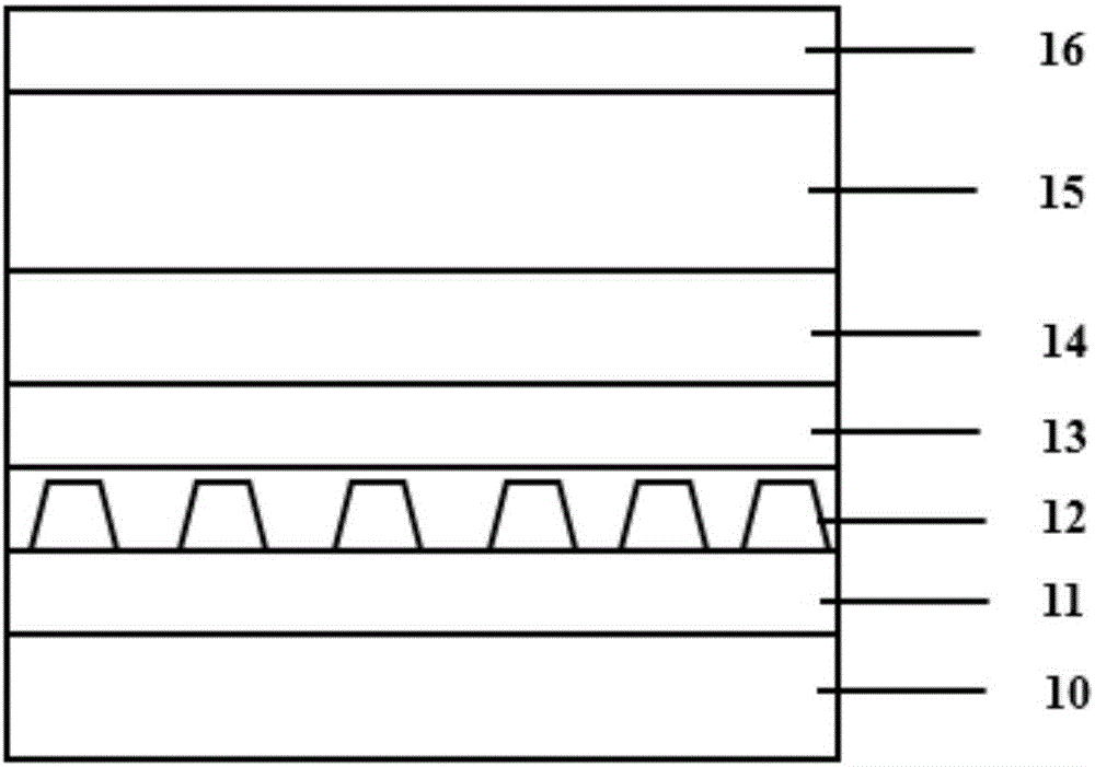
[0038] The preparation method of the LED epitaxial wafer grown on the magnesium scandium aluminate substrate of the present embodiment comprises the following steps:

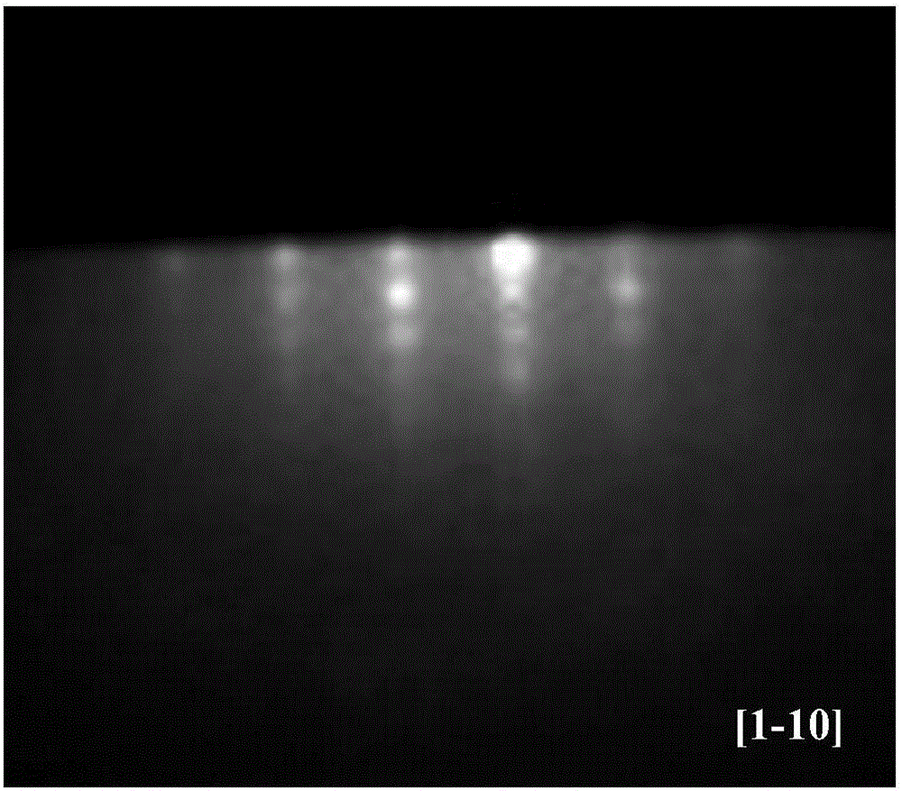
[0039] (1) Selection of the substrate and its crystal orientation: Magnesium aluminate scandium substrate is used, with the (0001) plane offset from the (11-20) plane by 0.5-1° as the epitaxial plane, and the crystal epitaxial orientation relationship is: (0001) of GaN ) plane parallel to ScMgAlO 4 (0001) face;

[0040] (2) Substrate annealing treatment, the specific process of the annealing is: the magnesium scandium aluminate substrate is annealed at 600° C. for 1 hour in the molecular beam epitaxy vacuum growth chamber of the substrate to obtain an atomically flat surface;

[0041] (3) GaN buffer layer epitaxial growth: the substrate temperature is adjusted to 450°C, and the pressure in the reaction chamber is 1.0×10 by pulsed laser deposition technology. -5 Pa, laser energy density is 2.0J / cm 2 A GaN buff...

Embodiment 2

[0053] The preparation method of the LED epitaxial wafer grown on the magnesium scandium aluminate substrate of the present embodiment comprises the following steps:

[0054] (1) Selection of the substrate and its crystal orientation: Magnesium aluminate scandium substrate is used, with the (0001) plane offset from the (11-20) plane by 0.5-1° as the epitaxial plane, and the crystal epitaxial orientation relationship is: (0001) of GaN ) plane parallel to ScMgAlO 4 (0001) face;

[0055] (2) Substrate annealing treatment, the specific process of the annealing is: annealing the magnesium scandium aluminate substrate at 700° C. for 2 hours in the molecular beam epitaxy vacuum growth chamber of the substrate to obtain an atomically flat surface;

[0056] (3) Epitaxial growth of GaN buffer layer: the substrate temperature is adjusted to 550°C, and the pressure in the reaction chamber is 4.0×10 by pulsed laser deposition technology. -5 Pa, laser energy density is 2.5J / cm 2 A GaN bu...


PUM

PropertyMeasurementUnit
Thicknessaaaaaaaaaa
Thicknessaaaaaaaaaa
Thicknessaaaaaaaaaa

Abstract

The invention discloses an LED epitaxial wafer grown on a magnesium aluminate scandium substrate. The LED epitaxial wafer comprises a GaN buffer layer grown on the magnesium aluminate scandium substrate, an Al nano island layer grown on the GaN buffer layer, a non-doped GaN layer grown on the Al nano island layer, an n-type doped GaN film grown on the non-doped GaN layer, an InGaN/GaN quantum well grown on the n-type doped GaN film and a p-type doped GaN film grown on the InGaN/GaN quantum well. The invention also discloses a preparation method of the LED epitaxial wafer grown on the magnesium aluminate scandium substrate The LED epitaxial wafer grown on the magnesium aluminate scandium substrate has the advantages of being simple in growth technology and low in preparation cost, and the prepared LED epitaxial wafer has smooth surface, low defect density and great photoelectric performance.

Description

technical field [0001] The invention relates to an LED epitaxial wafer and a preparation method thereof, in particular to an epitaxial wafer grown on scandium magnesium aluminate (ScMgAlO 4 ) LED epitaxial wafer on substrate and preparation method thereof. Background technique [0002] GaN and its related group III nitrides have excellent electrical, optical, and acoustic properties, and have been widely used in the preparation of light-emitting diodes (LEDs), laser diodes (LDs), and field-effect transistors. [0003] Commercial LEDs are mainly epitaxially grown on sapphire substrates. On the one hand, due to the lattice mismatch between sapphire and GaN as high as 13.3%, a high dislocation density is formed during the epitaxial GaN film process, which reduces the carrier mobility of the material and shortens the carrier lifetime, which ultimately affects performance of GaN-based devices. On the other hand, since the thermal mismatch between sapphire heat and GaN is as hi...

Claims


Application Information

Patent Timeline
IPC IPC(8): H01L33/00H01L33/32H01L33/06
CPCH01L33/0066H01L33/06H01L33/32H01L33/00
Inventor 李国强王文樑杨为家
Owner SOUTH CHINA UNIV OF TECH
Why Eureka
Try Eureka