Remote chip detection system of graphene probe sensing unit

A sensing unit and chip detection technology, applied in semiconductor/solid-state device testing/measurement, electrical components, single semiconductor device testing, etc., can solve problems such as inapplicability, achieve rapid detection, easy mass production and manufacturing, and reduce costs Effect

Active Publication Date: 2017-01-04
南京博泰测控技术有限公司
View PDF6 Cites 0 Cited by
  • Summary
  • Abstract
  • Description
  • Claims
  • Application Information

AI Technical Summary

Problems solved by technology

However, this scheme is not applicable in some occasions that require high precision

Method used


Image

  • Remote chip detection system of graphene probe sensing unit
  • Remote chip detection system of graphene probe sensing unit
  • Remote chip detection system of graphene probe sensing unit

Examples


Embodiment Construction

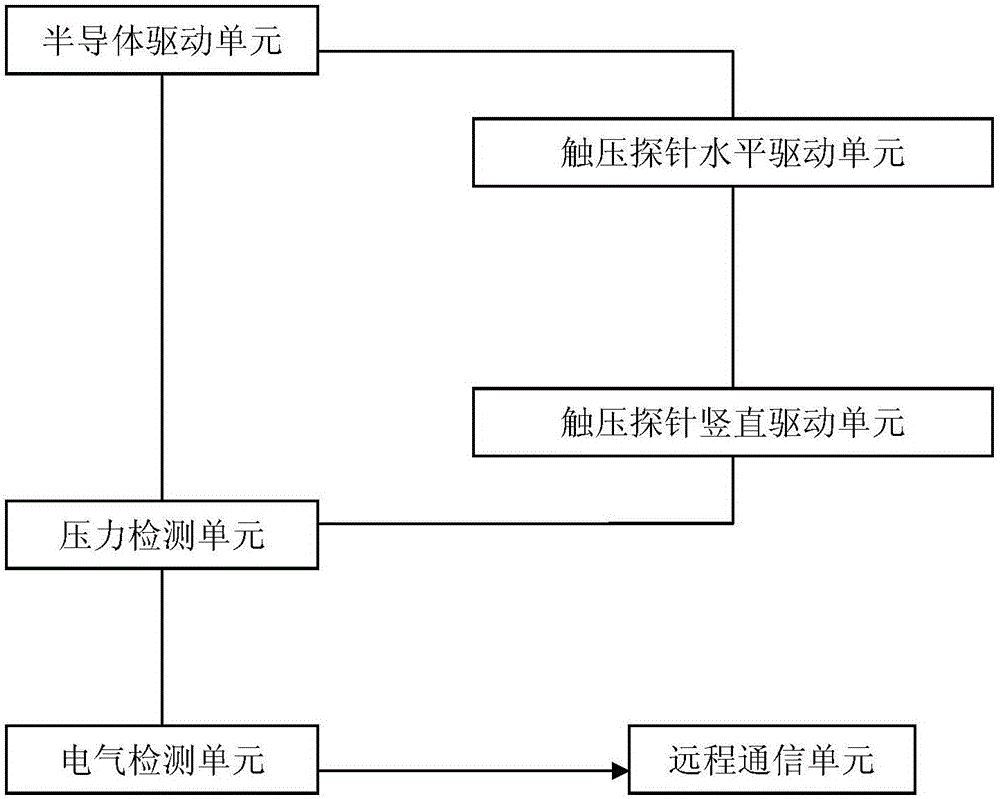
[0028] Such as figure 1 As shown, the remote chip detection system of the graphene probe sensing unit of the present invention includes: a semiconductor drive unit, a touch pressure probe horizontal drive unit, a touch pressure probe vertical drive unit, an electrical detection unit, a pressure detection unit and a remote The communication unit, the semiconductor drive unit, the touch probe horizontal drive unit and the touch probe vertical drive unit are connected in series by the drive signal line and driven sequentially, that is, the driving completion signal of the semiconductor drive unit is used as the The driving start signal of the horizontal driving unit of the touch pressure probe, the driving completion signal of the horizontal driving unit of the touch pressure probe is used as the driving start signal of the vertical driving unit of the touch pressure probe, and the pressure detection unit is The driving completion signal of the vertical driving unit of the contac...


PUM


Abstract

In order to realize high-accuracy semiconductor detection which does not need to be provided with an auxiliary structure like a pseudo gate electrode at lower cost, consider the automatic processing of a contact probe pressure signal level during a signal processing period and simultaneously carry out the transmission and the monitoring of a remote detection state, the invention provides a remote chip detection system of a graphene probe sensing unit. The remote chip detection system comprises a semiconductor driving unit, a horizontal driving unit of a contact probe, a vertical driving unit of the contact probe, an electric detection unit, a pressure detection unit and a remote communication unit, wherein the semiconductor driving unit, the horizontal driving unit of the contact probe and the vertical driving unit of the contact probe are mutually connected in series by a driving signal line and are driven in sequence; the pressure detection unit takes a driving finishing signal of the vertical driving unit of the contact probe as an initial signal of driving; a signal output by the pressure detection unit is input into the electric detection unit.

Description

technical field [0001] The invention relates to the technical field of semiconductor detection, and more specifically, to a remote chip detection system of a graphene probe sensing unit. Background technique [0002] With the rapid development of semiconductor manufacturing technology, in order to achieve faster computing speed, larger data storage capacity and more functions of semiconductor devices, semiconductor wafers are developing towards higher component density and high integration, and gates become Thinner and shorter in length than ever before. Therefore, the patterning accuracy for forming the gate is higher. In order to ensure the flatness of the surface, when forming the gate electrodes, it is preferable to form dummy gate electrodes so that the distribution of the gate electrodes is uniform. It is better to distribute dummy local interconnects when arranging via holes and local interconnect grooves, and such dummy structure regions are usually designed by aut...

Claims


Application Information

Patent Timeline
Patent Type & Authority Applications(China)
IPC IPC(8): G01R31/26H01L21/66
CPCG01R31/26H01L22/14
Inventor 刘颖
Owner 南京博泰测控技术有限公司
Why Eureka
Try Eureka