Forming method of semiconductor structure

A semiconductor and gas technology, applied in the direction of semiconductor devices, electrical components, circuits, etc., can solve the problems of low yield rate of IGBT, poor conductivity of silver metal layer electrodes, etc., and achieve the effect of improving conductivity

Inactive Publication Date: 2017-01-04
SEMICON MFG INT (SHANGHAI) CORP
View PDF4 Cites 0 Cited by
  • Summary
  • Abstract
  • Description
  • Claims
  • Application Information

AI Technical Summary

Problems solved by technology

[0005] In the actual process, the conductivity of the above-mentioned silver metal layer electrode is poor, resulting in a low yield of IGBT

Method used


Image

  • Forming method of semiconductor structure
  • Forming method of semiconductor structure
  • Forming method of semiconductor structure

Examples


Embodiment Construction

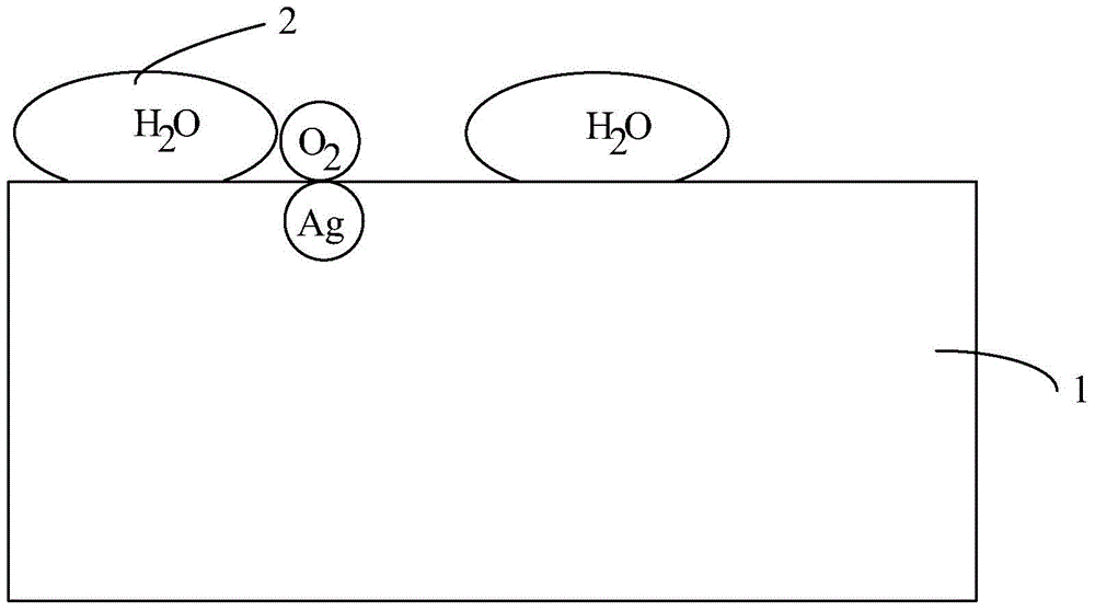
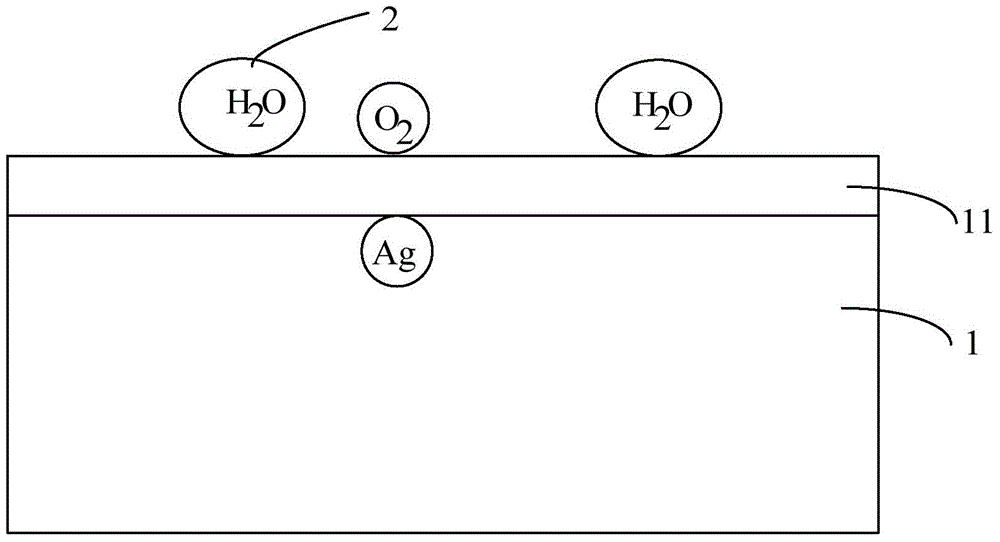
[0028] As described in the background art, in the prior art, the electrical conductivity of the silver metal layer electrode is poor. In view of the above problems, after analysis, it is found that the reasons for the problems are: figure 2 As shown in the figure, the silver atoms in the silver metal layer 1 can easily undergo redox reactions with oxygen in the air in a humid environment (high water vapor content and many water vapor particles 2) to generate Ag 2 O, resulting in white spots on the silver metal layer 1. At this time, conduct a conductivity test on the silver metal layer 1, if the probe is stuck on the Ag 2 On O (white spot), there will be a result that the conductivity test of the silver metal layer 1 fails. Therefore, it can be seen that Ag 2 O can reduce the electrical conductivity of the silver metal layer 1 . However, in a dry environment, it is difficult for silver atoms to undergo redox reactions with oxygen in the air to form Ag. 2 O.

[0029] Bas...


PUM


Abstract

The invention provides a forming method of a semiconductor structure. A deposited silver metal layer is processed by use of gaseous hexamethyl disilazane; and a layer of siloxane containing a methyl group is formed on the surface of the silicon metal layer. The siloxane has hydrophobicity and rejects attached water vapor particles, and the water vapor particles are in point contact on the siloxane. Compared with the condition that the water vapor particles are in surface contact on the surface of the unprocessed silver metal layer, the forming method provided by the invention has the advantage that the volume of water drops attached to the surface of the silver metal layer can be reduced, i.e., the adhesion amount of water vapor is reduced. The probability that Ag in the silver metal layer is combined with O2 in air under the condition of the water vapor to form Ag2O is reduced through reduction of the adhesion amount of the water vapor; and the conductivity of the silver metal layer is improved.

Description

technical field [0001] The present invention relates to the technical field of semiconductor manufacturing, and in particular, to a method for forming a semiconductor structure. Background technique [0002] In semiconductor integrated circuits, in order to reduce the resistance of some devices, it is necessary to use metallic silver to replace copper as an electrode, through which the electrical signal of the device can be extracted or applied to the device. [0003] Insulated Gate Bipolar Transistor (IGBT) is a commonly used vertical conduction type device. IGBT is a composite fully controlled voltage-driven power semiconductor device composed of BJT (Bipolar Transistor) and MOS (Insulated Gate Field Effect Transistor), which has both the high input impedance of MOSFET and the low on-voltage drop of GTR. The advantages. The BJT saturation voltage is reduced, the carrier density is large, but the driving current is large, the MOSFET driving power is small, and the switchi...

Claims


Application Information

Patent Timeline
Patent Type & Authority Applications(China)
IPC IPC(8): H01L21/28H01L29/417H01L29/739
CPCH01L29/401H01L29/41708H01L29/7398
Inventor 陈彧
Owner SEMICON MFG INT (SHANGHAI) CORP
Why Eureka
Try Eureka