LDMOS device and manufacturing method thereof

A device manufacturing method and device technology, which are used in semiconductor/solid-state device manufacturing, semiconductor devices, electrical components, etc., can solve the problem that the P-type layer is difficult to meet at the same time, and achieve reduced impact ionization, low on-resistance, and improved openness. The effect of state breakdown voltage

Active Publication Date: 2017-01-04
SHANGHAI HUAHONG GRACE SEMICON MFG CORP
View PDF4 Cites 6 Cited by
  • Summary
  • Abstract
  • Description
  • Claims
  • Application Information

AI Technical Summary

Problems solved by technology

Due to the different position of the strongest point of impact ionization in the on-state breakdown and off-state breakdown of the device, it is difficult for the P-type layer implanted with uniform doping to meet the requirements of ONBV and OFFBV at the same time.

Method used


Image

  • LDMOS device and manufacturing method thereof
  • LDMOS device and manufacturing method thereof
  • LDMOS device and manufacturing method thereof

Examples


Embodiment 1

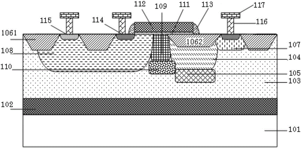
[0062] Such as figure 1 As shown, the LDMOS device includes a P-type epitaxial layer 103, an N well 107, a P well 108, a first N-type drift region 104, a first P-type layer 105, a second N-type drift region 109, a second P-type layer 110, Gate oxide layer 111, gate polysilicon 112;

[0063] The P-well 108, the second N-type drift region 109, the first N-type drift region 104, and the N-well 107 are successively formed on the upper part of the P-type epitaxial layer 103 from left to right;

[0064] The gate oxide layer 111 is formed on the right part of the P well 108, the left part of the first N-type drift region 104 and above the second N-type drift region 109;

[0065] The gate polysilicon 112 is formed on the gate oxide layer 111;

[0066] The second N-type drift region 109 is shallower than the first N-type drift region 104;

[0067] The second P-type layer 110 and the first P-type layer 105 are formed in the P-type epitaxial layer 103;

[0068] The second P-type laye...

Embodiment 2

[0076] Based on the LDMOS device of the first embodiment, the N-type doping concentration of the first N-type drift region 104 and the second N-type drift region 109 is smaller than the N-type doping concentration of the N-well 107 .

[0077] Preferably, the N-type doping concentration of the first N-type drift region 104 and the second N-type drift region 109 is within 1e 16 / cm 3 to 5e 16 / cm 3 between.

[0078] In the LDMOS device of the second embodiment, the N-type drift region is lightly doped, which can increase the breakdown voltage of the PN junction between the N well 107 and the P well 108 .

Embodiment 3

[0080] Based on the LDMOS device of Embodiment 1, a field oxide 1062 in a field oxide region is formed above the first N-type drift region 104;

[0081] The gate oxide layer 111 is formed on the right part of the P well 108, the left part of the field oxide region 1062 and above the second N-type drift region 109;

[0082] There is a trench isolation region isolation oxide 1061 between the N-type heavily doped region 114 and the P-type heavily doped region 115 formed on the P well 108;

[0083] The trench isolation region isolation oxide 1061 is deeper than the field oxide region 1062 .

[0084] The LDMOS device of Embodiment 3 can be integrated in the BCD process, and the N-type drift region and the P-type layer are implanted on the bottom of the ultra-shallow trench in the field oxygen region using the mask plate etched by the ultra-shallow trench, and then the conventional isolation is formed. Trench, because the ultra-shallow trench isolation is carried out separately fro...


PUM


Abstract

The invention discloses an LDMOS device which comprises a P-type epitaxial layer, an N-well, a P-well, a first N-type drift region, a first P-type layer, a second N-type drift region, a second P-type layer, a gate oxide layer and gate polysilicon. The P-well, the second N-type drift region, the first N-type drift region and the N-well are sequentially contiguous from left to right at the upper part of the P-type epitaxial layer. The second N-type drift region is shallower than the first N-type drift region. The second P-type layer is adjacent to the lower part of the second N-type drift region. The first P-type layer is adjacent to the lower part of the first N-type drift region. The second P-type layer is shallower than the first P-type layer. The second P-type layer has a higher doping concentration than the first P-type layer. The invention further discloses a manufacturing method for the LDMOS device. According to the invention, the LDMOS device has lower on-resistance, and can satisfy off-state breakdown voltage and on-state breakdown voltage at the same time.

Description

technical field [0001] The invention relates to semiconductor technology, in particular to an LDMOS device and a manufacturing method thereof. Background technique [0002] LDMOS (Lateral Diffused Medal Oxide Semiconductor, Lateral Diffused Metal Oxide Semiconductor) transistor is widely used as a power MOS transistor because it is easier to be compatible with the CMOS process. [0003] In LDMOS devices, on-resistance (Rdson), off-state breakdown voltage (OFFBV) and on-state breakdown voltage (ONBV) are important indicators. [0004] In order to make high-performance LDMOS, it is usually necessary to add an additional N-type implant in the drift region of the device to make the device have a lower on-resistance. In order to obtain a competitive on-resistance, the N-type implant dose should be as large as possible , and using this method will reduce the device's off-state breakdown voltage (OFFBV). [0005] In order to improve the off-state breakdown voltage (OFFBV) of the ...

Claims


Application Information

Patent Timeline
Patent Type & Authority Applications(China)
IPC IPC(8): H01L29/78H01L21/336H01L29/10H01L29/06
CPCH01L29/0611H01L29/1083H01L29/66681H01L29/7816
Inventor 石晶
Owner SHANGHAI HUAHONG GRACE SEMICON MFG CORP
Why Eureka
Try Eureka