Preparation method for VDMOS integrated ESD structure

An epitaxial layer and process technology, which is applied in the field of preparation of VDMOS integrated ESD structures, can solve problems such as increased step difference, process difficulty, and large step height difference, and achieves reduced step height difference, convenient process, and improved device durability. pressure effect

Inactive Publication Date: 2017-01-04
XIAN LONTEN RENEWABLE ENERGY TECH
View PDF3 Cites 11 Cited by
  • Summary
  • Abstract
  • Description
  • Claims
  • Application Information

AI Technical Summary

Problems solved by technology

In this way, the epitaxial layer at the position of the active region is lost in the field oxygen growth, which reduces the withstand voltage capability of the entire epitaxial structure
[0004] 2. The method of directly growing field oxygen. After forming the field oxygen pattern, all the field oxygen is located on the surface of the epitaxial layer, which leads to a large step height difference between the active region and the epitaxial surface. After the polysilicon is deposited in the later process The step difference is further increased, which affects the flatness of the silicon wafer surface and brings difficulty to the subsequent process, especially the process using dielectric CMP is more difficult.

Method used


Image

  • Preparation method for VDMOS integrated ESD structure
  • Preparation method for VDMOS integrated ESD structure
  • Preparation method for VDMOS integrated ESD structure

Examples


Embodiment Construction

[0039] In order to make the object, technical solution and advantages of the present invention clearer, the present invention will be further described in detail below in conjunction with the accompanying drawings and embodiments. It should be understood that the specific embodiments described here are only used to explain the present invention, not to limit the present invention.

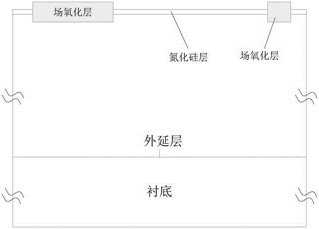
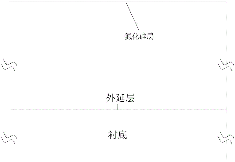
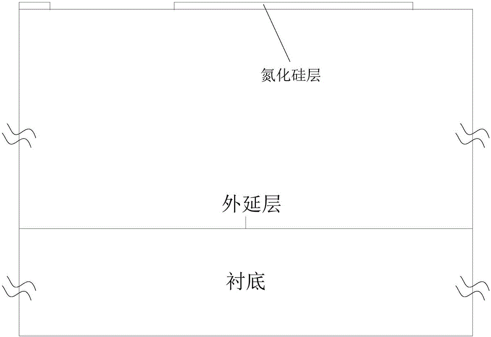
[0040] An embodiment of the present invention is a method for preparing a VDMOS integrated ESD structure. The method is: forming a pattern by silicon nitride deposition and photolithography etching, growing a field oxide layer in the area where the epitaxial layer is exposed after the silicon nitride is etched away, and then The ESD structure is completed in the follow-up and traditional VDMOS process.

[0041] The embodiment of the present invention provides a method for preparing a VDMOS integrated ESD structure, the method is realized through the following steps:

[0042] Step 1: Provide an n-t...


PUM


Abstract

The invention discloses a preparation method for a VDMOS integrated ESD structure, and the method comprises the steps: forming an epitaxial layer on a substrate; depositing a silicon nitride layer on the surface of the epitaxial layer, presetting a grid region or a terminal as an ESD region through employing the photoetching technology and the dry etching technology, etching the ESD region, enabling the epitaxial layer to be exposed in a part of the region, and enabling the remaining region to be still covered by the silicon nitride layer; growing a field oxide layer in the region where the epitaxial layer is exposed through the boiler tube technology; carrying out the wet etching of silicon nitride layer, and keeping a field oxide pattern; forming a trench in an active region; forming MOSFET device gate oxide; depositing polycrystalline silicon; forming polycrystalline silicon patterns of a device grid and an ESD PN junction; forming a P well; completing the junction injection of the PN junction on the ESD polycrystalline silicon pattern while forming a device source electrode, and forming an ESD; depositing a medium; forming a lead wire hole; completing hole tungsten filling and surface metal technology, and forming a device front structure; and finally forming a final device structure. The method avoids the loss of an active region epitaxial layer in the growth of a thermal oxidation layer, and increases the withstand voltage of a device.

Description

technical field [0001] The invention relates to the field of semiconductor integrated circuit manufacturing, in particular to a method for preparing a VDMOS integrated ESD structure. Background technique [0002] Existing ESD preparation process structure and process: [0003] 1. After the epitaxial preparation, a very thick field oxide layer is directly grown on the epitaxial layer. Then use photolithography to form the required pattern, and wet-etch away the field oxygen in the redundant position. In this way, the epitaxial layer at the position of the active region is lost in the field oxygen growth, which reduces the withstand voltage capability of the entire epitaxial structure. [0004] 2. The method of directly growing field oxygen. After forming the field oxygen pattern, all the field oxygen is located on the surface of the epitaxial layer, which leads to a large step height difference between the active region and the epitaxial surface. After the polysilicon is de...

Claims


Application Information

Patent Timeline
Patent Type & Authority Applications(China)
IPC IPC(8): H01L29/78H01L21/336
CPCH01L29/7802H01L29/66712
Inventor 岳玲刘挺杨乐周宏伟徐西昌
Owner XIAN LONTEN RENEWABLE ENERGY TECH
Why Eureka
Try Eureka