Transparent glass-based double-layer circuit board

A double-layer circuit board, glass substrate technology, applied in the direction of transparent dielectrics, circuit substrate materials, printed circuits, etc., can solve the problem that the conductive layer and the insulating layer are not closely connected, the conductive layer is easily damaged and peeled off, and the surface of the circuit board is not smooth, etc. problems, to achieve the effect of maintaining superconductivity, surface smoothness, and preventing surface oxidation

Active Publication Date: 2017-01-04
WUHAN HSURICH TECH CO LTD
View PDF5 Cites 2 Cited by
  • Summary
  • Abstract
  • Description
  • Claims
  • Application Information

AI Technical Summary

Problems solved by technology

[0004] However, the epoxy glass or polyimide material of the double-sided wiring printed circuit board is used as the insulating layer, and the conductive layer is the copper foil pasted on the surface of the insulating layer. Since the bonding effect of the adhesive gradually decreases after long-term use, so It will lead to loose connection between the conductive layer and the insulating layer, the conductive layer floats on the surface of the glass plate, the surface of the entire circuit board is not smooth, the conductive layer is easily damaged and falls off, and eventually leads to poor conduction ability; and the overall thickness of the circuit board is relatively large In order to make the copper foil thinner, although the extremely thin copper foil material is used as much as possible, the current situation is still that its limit reaches a thickness of about 12um.

Method used


Image

  • Transparent glass-based double-layer circuit board
  • Transparent glass-based double-layer circuit board
  • Transparent glass-based double-layer circuit board

Examples


Embodiment 1

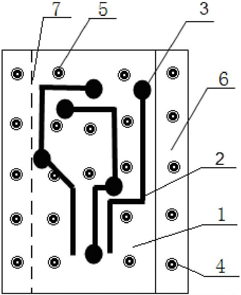
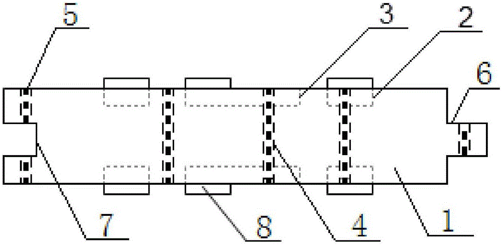
[0024] Embodiment 1: a kind of transparent glass-based double-layer circuit board, its structure is as follows figure 1 and figure 2 As shown, including a glass substrate 1, the glass substrate is a toughened glass plate, and the glass substrate 1 is evenly distributed with conduction holes 4 penetrating the glass substrate. Thick hollow copper tube 5, the end face of the hollow copper tube is flush with the surface of the glass substrate; the upper surface and the lower surface of the glass substrate are provided with conductive lines 2 that are fused with the surface of the glass substrate, and the conductive lines 2 are graphene , the surface of the conductive line 2 except the pad 3 of the component to be welded is covered with PCB organic solder resist varnish 8, the two conductive lines form electrical conduction through the hollow copper tube, and the surface of the glass substrate is flush with the upper surface of the conductive line; The middle part of one side of ...

Embodiment 2

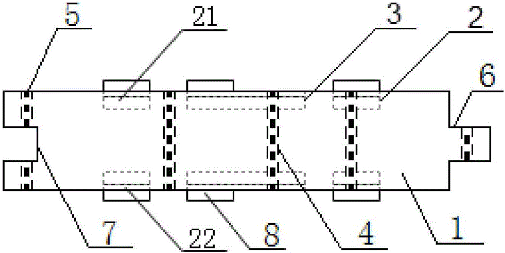
[0025] Embodiment 2: a kind of transparent glass-based double-layer circuit board, its structure is as figure 1 and image 3 As shown, including a glass substrate 1, the glass substrate is a toughened glass plate, and the glass substrate 1 is evenly distributed with conduction holes 4 penetrating the glass substrate. thick hollow copper tube 5, the end face of the hollow copper tube is flush with the surface of the glass substrate; the upper and lower surfaces of the glass substrate are provided with conductive lines 2 that are fused with the surface of the glass substrate, and the conductive lines 2 are formed by the surface The graphene layer 22 and the conductive layer formed by the metal layer 21 fused with the glass substrate at the bottom layer, and the contact surface between the graphene layer 22 and the metal layer 21 are mutually fused, and the pad 3 of the component to be welded is removed from the surface of the conductive circuit 2 The other part is covered with ...


PUM

PropertyMeasurementUnit
diameteraaaaaaaaaa

Abstract

The invention provides a transparent glass-based double-layer circuit board. The circuit board includes a glass substrate which is evenly distributed thereon with electric guide holes which penetrate the glass substrate. Each electric guide hole is provided with a hollow copper tube therein with a length equal to the thickness of the glass substrate. An end surface of the hollow copper tube is level with the surface of the glass substrate. The upper surface and the lower surface of the glass substrate are both provided with a conducting circuit which is fused with the surface of the glass substrate. The two conducting circuits are electrically on through the hollow copper tubes. Each conducting circuit is made of graphene, or a conducting layer constituted by a surface layer which is graphene and a bottom layer which is a layer fused with the glass substrate, and the contact surfaces of the graphene and the metal are fused mutually. According to the invention, the circuit board adopts tempered glass as an insulation plate, by fused fixing of the conducting circuits on the upper surface and the lower surface of the glass substrate, achieves the formation of a double layer, can increase the carrying capacity of an electric element by one time than traditional glass substrate having the same area, and greatly reduces the size of a circuit board.

Description

technical field [0001] The invention relates to a double-layer circuit board, in particular to a transparent glass-based double-layer circuit board, which belongs to the technical field of electronic devices. Background technique [0002] As a national pillar industry, the electronics industry has developed rapidly in recent years, especially for terminal products that are light, thin, short, and small. For its basic industry—the printed circuit board industry, it has proposed high-density, small-volume, Higher requirements such as high conductivity. Circuit board technology has developed rapidly under this background, and industries in various weak current fields, such as computers and peripheral auxiliary systems, medical equipment, mobile phones, digital (camera) cameras, communication equipment, precision instruments, aerospace, etc. The process and quality of printed circuit boards have put forward many specific and clear technical specifications. [0003] With the ra...

Claims


Application Information

Patent Timeline
Patent Type & Authority Applications(China)
IPC IPC(8): H05K1/03H05K3/38
CPCH05K1/0306H05K3/382H05K2201/0108
Inventor 尤晓江
Owner WUHAN HSURICH TECH CO LTD
Why Eureka
Try Eureka