Top gate type thin film transistor and production method thereof

A technology of thin film transistors and manufacturing methods, which is applied in the direction of transistors, semiconductor/solid-state device manufacturing, semiconductor devices, etc., can solve problems such as surface damage of metal oxide semiconductor materials, unstable resistance of source and drain regions, and influence on device stability, etc., to achieve The effect of stable resistance, light surface damage and stable performance

Inactive Publication Date: 2017-01-25
SHENZHEN CHINA STAR OPTOELECTRONICS TECH CO LTD
View PDF3 Cites 13 Cited by
  • Summary
  • Abstract
  • Description
  • Claims
  • Application Information

AI Technical Summary

Problems solved by technology

[0006] The current preparation methods of top-gate thin film transistors include: metal doping, ion implantation, plasma treatment, deposition of hydrogenated silicon nitride for hydrogen doping and other methods; however, these methods have more or less disadvantages, for example, The method of metal doping needs to add a film forming process and an annealing process; the method of ion implantation is easy to cause damage to the surface of the metal oxide semiconductor material, and increases the process cost; the method of plasma treatment is easy to cause damage to the surface of the metal oxide semiconductor material , and after the annealing process, the resistance of the source and drain regions is unstable and easy to rise; finally, the method of depositing hydrogenated silicon nitride for hydrogen doping reduces the metal oxide semiconductor material, and the free hydrogen atoms easily affect the stability of the device sex

Method used


Image

  • Top gate type thin film transistor and production method thereof
  • Top gate type thin film transistor and production method thereof
  • Top gate type thin film transistor and production method thereof

Examples


Embodiment Construction

[0036] In order to further illustrate the technical means adopted by the present invention and its effects, the following describes in detail in conjunction with preferred embodiments of the present invention and accompanying drawings.

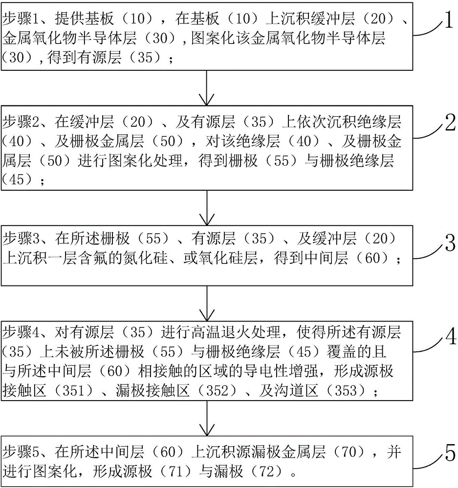
[0037] see figure 1 , the invention provides a method for manufacturing a top-gate thin film transistor, comprising the following steps:

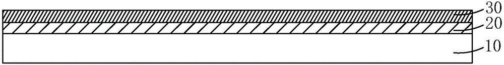
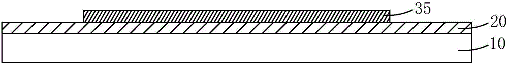
[0038] Step 1, such as Figure 2-3 As shown, a substrate 10 is provided, a buffer layer 20 and a metal oxide semiconductor layer 30 are sequentially deposited on the substrate 10 , and the metal oxide semiconductor layer 30 is patterned to obtain an active layer 35 .

[0039] Specifically, the buffer layer 20 is formed by depositing insulating materials such as silicon oxide and silicon nitride.

[0040] Specifically, the metal oxide semiconductor layer 30 is formed by depositing at least one of zinc oxide-based, indium oxide-based, tin oxide-based and other semiconductor materials.

[0041] Step 2, such...


PUM


Abstract

The invention provides a method for manufacturing a top-gate thin film transistor and the top-gate thin film transistor. In the manufacturing method of the top-gate thin film transistor of the present invention, while depositing and forming the intermediate layer, doping it with fluorine element, and then using the gate and the gate insulating layer as shields, performing high-temperature annealing treatment on the active layer, and Under the action of the intermediate layer, after the high-temperature annealing treatment, the metal oxide semiconductor material in the region of the active layer that is not covered by the gate and the gate insulating layer and is in contact with the intermediate layer is covered with fluorine ions. Compared with the traditional production method, this method does not need to add new process steps, and the surface damage to the metal oxide semiconductor material in the source and drain contact areas is relatively light, and at the same time, it can effectively reduce the source and drain contact area. The resistance of the region, and the resistance of the source and drain contact regions after high-temperature annealing is stable, and will not affect the stability of the device.

Description

technical field [0001] The invention relates to the field of display technology, in particular to a method for manufacturing a top-gate thin film transistor and the top-gate thin film transistor. Background technique [0002] In the field of display technology, flat panel display devices are widely used in mobile phones, televisions, personal digital assistants, digital cameras, notebook computers, desktop computers, etc. Various consumer electronic products have become the mainstream of display devices. [0003] Thin Film Transistor (TFT) is currently the main driving element in Liquid Crystal Display (LCD) and Active Matrix Organic Light-Emitting Diode (AMOLED). It is directly related to the development direction of high-performance flat panel display devices. [0004] Thin film transistors have various structures, and there are various materials for preparing the active layer of thin film transistors with corresponding structures. Among them, metal oxide thin film trans...

Claims


Application Information

Patent Timeline
Patent Type & Authority Applications(China)
IPC IPC(8): H01L21/336H01L29/786
CPCH01L29/66969H01L29/7869
Inventor 刘洋
Owner SHENZHEN CHINA STAR OPTOELECTRONICS TECH CO LTD
Why Eureka
Try Eureka