InGaN/GaN nano-pillar multiple quantum well grown on strontium tantalum lanthanum aluminate substrate and preparation method thereof
A technology of strontium aluminate tantalum lanthanum and multiple quantum wells, which is applied in electrical components, circuits, semiconductor devices, etc., can solve the problems of chemical instability and other problems, and achieve the effects of easy acquisition, reduction of dislocation formation, and elimination of adverse effects
- Summary
- Abstract
- Description
- Claims
- Application Information
AI Technical Summary
Problems solved by technology
Method used
Image
Examples
Embodiment 1
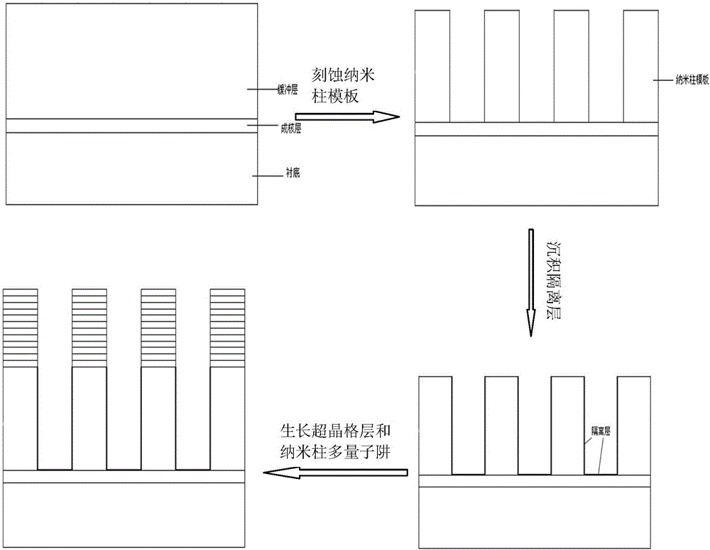
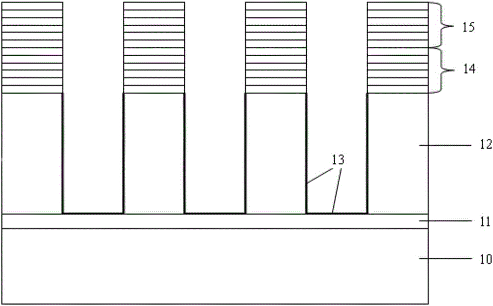
[0041] The preparation method of the InGaN / GaN nanocolumn multiple quantum well grown on the strontium tantalum lanthanum aluminate substrate of this embodiment comprises the following steps:
[0042] (1) Selection of the substrate and its crystal orientation: using La 0.3 Sr 1.7 AlTaO 6 The substrate, with the (111) plane offset from the (100) direction by 0.5-1° as the epitaxial plane, the crystal epitaxial orientation relationship is: the (0001) plane of GaN is parallel to the La 0.3 Sr 1.7 AlTaO 6 (111) side;
[0043] (2) Substrate surface polishing, cleaning and annealing treatment, the specific process of the annealing is: put the substrate into the annealing chamber, and treat La 0.3 Sr 1.7 AlTaO 6 The substrate was annealed for 3 hours and then air-cooled to room temperature;
[0044] The surface polishing of the substrate is specifically: firstly La 0.3 Sr 1.7 AlTaO 6 The surface of the substrate is polished with diamond slurry, and the surface of the subst...
Embodiment 2
[0055] The preparation method of the nanocolumn LED grown on the strontium tantalum lanthanum aluminate substrate of this embodiment comprises the following steps:
[0056] (1) Selection of the substrate and its crystal orientation: using La 0.3 Sr 1.7 AlTaO 6 The substrate, with the (111) plane offset from the (100) direction by 0.5-1° as the epitaxial plane, the crystal epitaxial orientation relationship is: the (0001) plane of GaN is parallel to the La 0.3 Sr 1.7 AlTaO 6 (111) side;
[0057] (2) Substrate surface polishing, cleaning and annealing treatment, the specific process of the annealing is: put the substrate into the annealing chamber, and treat La 0.3 Sr 1.7 AlTaO 6 The substrate was annealed for 5 hours and then air-cooled to room temperature;
[0058]The surface polishing of the substrate is specifically:
[0059] La 0.3 Sr 1.7 AlTaO 6 The surface of the substrate is polished with diamond slurry, and the surface of the substrate is observed with an op...
PUM
| Property | Measurement | Unit |
|---|---|---|
| thickness | aaaaa | aaaaa |
| height | aaaaa | aaaaa |
| diameter | aaaaa | aaaaa |
Abstract
Description
Claims
Application Information
 - R&D
- Intellectual Property
- Life Sciences
- Materials
- Tech Scout
- Unparalleled Data Quality
- Higher Quality Content
- 60% Fewer Hallucinations
Browse by: Latest US Patents, China's latest patents, Technical Efficacy Thesaurus, Application Domain, Technology Topic, Popular Technical Reports.
© 2025 PatSnap. All rights reserved.Legal|Privacy policy|Modern Slavery Act Transparency Statement|Sitemap|About US| Contact US: help@patsnap.com


