

LED epitaxial layer growth method
A growth method and epitaxial layer technology, applied in electrical components, circuits, semiconductor devices, etc., can solve the problems of N-electrode, P-electrode asymmetry, uneven current dispersion of light-emitting layer, uneven light-emitting area, etc., to achieve the distribution of current The effect of uniformity, increased luminous efficiency, and strong trapping effect
- Summary
- Abstract
- Description
- Claims
- Application Information
AI Technical Summary
Problems solved by technology
Method used
Image

Examples
Embodiment 1
[0047] The invention uses MOCVD to grow high-brightness GaN-based LED epitaxial wafers. Using high-purity H 2 or high purity N 2 or high purity H 2 and high purity N 2 The mixed gas as the carrier gas, high-purity NH 3 As the N source, the metal-organic source trimethylgallium (TMGa) is used as the gallium source, trimethylindium (TMIn) is used as the indium source, and the N-type dopant is silane (SiH 4 ), trimethylaluminum (TMAl) as the aluminum source, and the P-type dopant as magnesium dicene (CP 2 Mg), the substrate is (001) sapphire, and the reaction pressure is between 70mbar and 900mbar. The specific growth method is as follows:
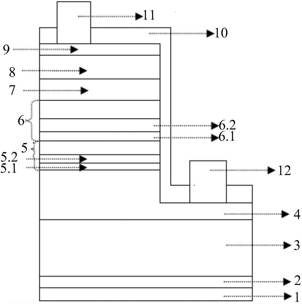
[0048] A kind of LED epitaxial layer growth method, epitaxial structure see figure 1 , including: processing the substrate, growing a low-temperature buffer layer GaN, growing an undoped GaN layer, growing a Si-doped N-type GaN layer, growing a light-emitting layer, growing a P-type AlGaN layer, and growing a Mg-doped P-type GaN layer ...
Embodiment 2
[0057] The application examples of the LED epitaxial layer growth method of the present invention are provided below, and its epitaxial structure can be found in figure 1 . Using MOCVD to grow high-brightness GaN-based LED epitaxial wafers. Using high-purity H 2 or high purity N 2 or high purity H 2 and high purity N 2 The mixed gas as the carrier gas, high-purity NH 3 As the N source, the metal-organic source trimethylgallium (TMGa) is used as the gallium source, trimethylindium (TMIn) is used as the indium source, and the N-type dopant is silane (SiH 4 ), trimethylaluminum (TMAl) as the aluminum source, and the P-type dopant as magnesium dicene (CP 2 Mg), the substrate is (0001) sapphire, and the reaction pressure is between 70mbar and 900mbar. The specific growth method is as follows:
[0058] Step 101, processing the substrate:
[0059] H at 1000°C-1100°C 2 Under the atmosphere, feed 100L / min-130L / min of H 2 , keep the reaction chamber pressure at 100mbar-300mba...
Embodiment 3
[0084] A conventional LED epitaxial growth method is provided below as a comparative example of the present invention.
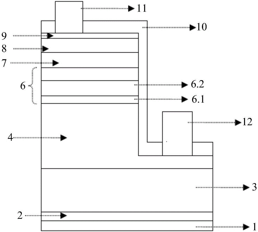
[0085] The growth method of conventional LED epitaxy is (see the epitaxial layer structure figure 2 ):
[0086] 1. H at 1000°C-1100°C 2 Under the atmosphere, feed 100L / min-130L / min of H 2 , keep the reaction chamber pressure at 100mbar-300mbar, and process the sapphire substrate for 8min-10min.
[0087] 2. Lower the temperature to 500°C-600°C, keep the reaction chamber pressure at 300mbar-600mbar, and feed the flow rate at 10000sccm-20000sccm NH 3 , 50sccm-100sccm TMGa, 100L / min-130L / min H 2 , grow a low-temperature buffer layer GaN with a thickness of 20nm-40nm on a sapphire substrate.
[0088] 3. Raise the temperature to 1000°C-1200°C, keep the pressure in the reaction chamber at 300mbar-600mbar, and feed NH with a flow rate of 30000sccm-40000sccm 3 , 200sccm-400sccm TMGa, 100L / min-130L / min H 2 , Continuous growth of 2μm-4μm undoped GaN layer.
[...
PUM
| Property | Measurement | Unit |
|---|---|---|
| Luminous wavelength | aaaaa | aaaaa |
Abstract
Description
Claims
Application Information