Deep-groove PCB board and processing method thereof

A PCB board and processing method technology, applied in the field of deep groove PCB board and its processing, can solve the problems of easily damaged copper layer, groove edge warping, low processing efficiency, etc., so as to avoid warping and improve processing accuracy , The effect of improving processing efficiency

Inactive Publication Date: 2017-02-15
SHENZHEN KINWONG ELECTRONICS
View PDF6 Cites 2 Cited by
  • Summary
  • Abstract
  • Description
  • Claims
  • Application Information

AI Technical Summary

Problems solved by technology

[0004] In view of the above-mentioned deficiencies in the prior art, the object of the present invention is to provide a deep groove PCB board and its processing method, aiming to solve the problems of easy damage to the copper layer, low processing efficiency, and easy occurrence of deep groove PCB processing methods in the existing deep groove PCB. The problem of groove edge warping phenomenon

Method used


Image

  • Deep-groove PCB board and processing method thereof
  • Deep-groove PCB board and processing method thereof
  • Deep-groove PCB board and processing method thereof

Examples


Embodiment Construction

[0028] The present invention provides a deep-groove PCB board and its processing method. In order to make the purpose, technical solution and effect of the present invention clearer and clearer, the present invention will be further described in detail below. It should be understood that the specific embodiments described here are only used to explain the present invention, not to limit the present invention.

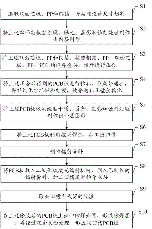
[0029] see figure 1 , figure 1 It is a flow chart of a preferred embodiment of the processing method of a deep groove PCB board of the present invention, as shown in the figure, which includes:

[0030] Step S1, material cutting: select double-sided core board, PP and copper foil, and cut according to the designed size;

[0031] Step S2, making inner layer graphics: making the inner layer graphics by coating, exposing, developing and etching the above-mentioned double-sided core board;

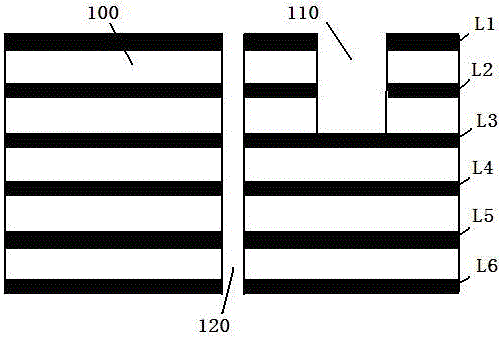
[0032] Step S3, lamination: Laminate the above double-sided core board, PP and c...


PUM


Abstract

The invention discloses a deep-groove PCB board and a processing method thereof. The method comprises the following steps: step E, manufacturing an outer graph; orderly pasting a dry film, exposing, developing and etching on a PCB board to manufacture the outer graph; F, groove gonging: processing a groove on the PCB board by use of a depth-controlling gong machine; G, manufacturing laser document: manufacturing the laser document; H, forming the groove: placing the PCB board in a carbon dioxide laser machine, invoking the manufactured laser document to process a dielectric layer on the groove bottom; I, removing adhesive: removing residual adhesive slag in the groove; J, solder masking and surface processing: silk-printing solder-masking printing ink on the adhesive-removed PCB board to form a solder masking layer; and then forming a deep-groove PCB board through gold-immersion surface processing. Through the adoption of the method disclosed by the invention, the groove processing precision of the PCB board is improved to prevent a copper layer from being damaged in the groove processing procedure of the PCB board; and meanwhile, the processing efficiency is improved to prevent the groove side warping phenomenon from occurring.

Description

technical field [0001] The invention relates to the field of PCB boards, in particular to a deep groove PCB board and a processing method thereof. Background technique [0002] There are generally two methods for processing PCB grooves: one is to use a depth-controlling machine with a depth-controlling function to process the grooves by controlling the depth. Using this method, the depth-control accuracy is about ±0.1mm, but this processing accuracy It is easy to damage the copper layer; the other is to use UV laser equipment to cut the groove. This method has low processing efficiency because the UV laser spot is only 25 μm. In addition, the edge of the groove is prone to warping during processing. [0003] Therefore, the prior art still needs to be improved and developed. Contents of the invention [0004] In view of the above-mentioned deficiencies in the prior art, the object of the present invention is to provide a deep groove PCB board and its processing method, aim...

Claims


Application Information

Patent Timeline
Patent Type & Authority Applications(China)
IPC IPC(8): H05K3/46
CPCH05K3/4611H05K2203/02H05K2203/107
Inventor 刘羽付凤奇王俊陆玉婷邝美娟田晓燕
Owner SHENZHEN KINWONG ELECTRONICS
Why Eureka
Try Eureka