High-reliability surface mounted rectification chip

A rectifier chip and reliability technology, applied in the direction of electrical components, electrical solid devices, circuits, etc., can solve problems such as product electrical or reliability failures, avoid product yield loss, reduce manufacturing costs, and improve product electrical properties and reliability effects

Active Publication Date: 2017-02-22
SUZHOU GOODARK ELECTRONICS CO LTD
View PDF3 Cites 0 Cited by
  • Summary
  • Abstract
  • Description
  • Claims
  • Application Information

AI Technical Summary

Problems solved by technology

During the molding process, injection molding pores are prone to appear inside the product. These pores can lead to electrical or reliability failure of the product. Therefore, how to develop a semiconductor packaging structure that is easy to locate and can solve the above problems has become the direction of efforts of those skilled in the art.

Method used


Image

  • High-reliability surface mounted rectification chip
  • High-reliability surface mounted rectification chip
  • High-reliability surface mounted rectification chip

Examples


Embodiment

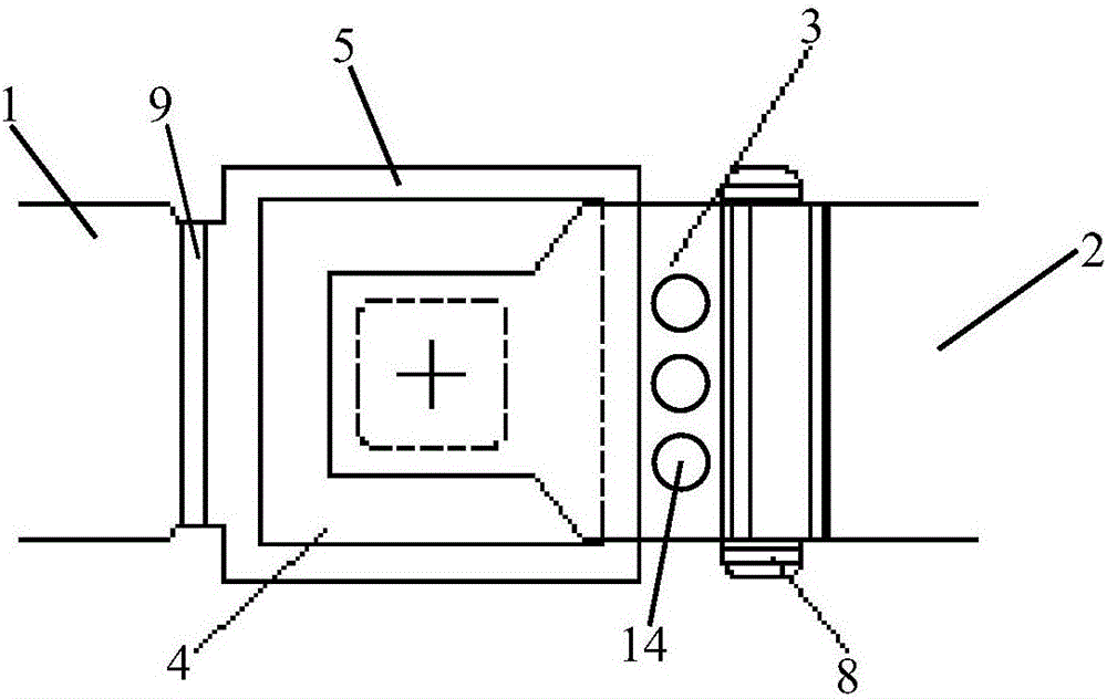
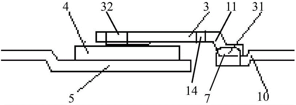
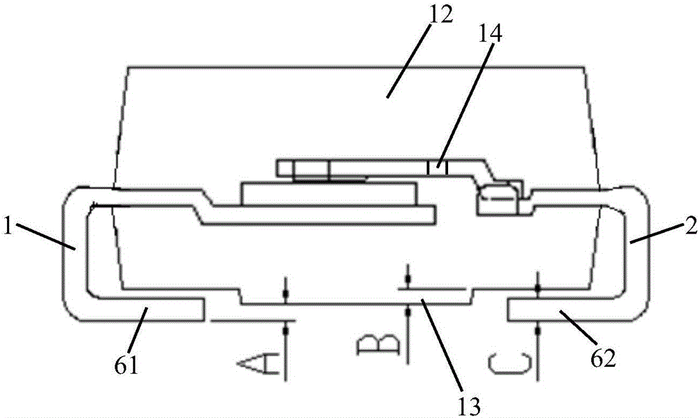
[0023] Embodiment: a kind of high-reliability SMD rectifier chip, as attached Figure 1~3 As shown, it includes a first lead bar 1, a second lead bar 2, a connecting sheet 3 and a diode chip 4 located in an epoxy package 12, and one end of the first lead bar 1 is a support area 5 connected to the diode chip 4, One end of the diode chip 4 is electrically connected to the support area 5 through solder paste, and the other end of the first lead bar 1 is a pin area 61, and the pin area 61 of the first lead bar 1 is used as the current transmission end of the rectifier;

[0024] One end of the second lead bar 2 is a welding area 7 connected to the first welding end 31 of the connecting piece 3, the other end of the second lead bar 2 is a pin area 62, and the pin of the second lead bar 2 zone 62 as the current transfer terminal of the rectifier;

[0025] The second welding end 32 of the connecting piece 3 is electrically connected to the other end of the diode chip 4 through solder...


PUM


Abstract

The invention provides a high-reliability surface mounted rectification chip comprising a first lead strip, a second lead strip, a connecting sheet and a diode chip which are arranged in an epoxy packaging body. A first bending part is arranged in the area between the supporting area and the pin area of the first lead strip so that the supporting area of the first lead strip is enabled to be lower than the pin area. A second bending part is arranged in the area between the welding area and the pin area of the second lead strip so that the welding area of the second lead strip is enabled to be lower than the pin area. A third bending part is arranged between the first welding end and the second welding end of the connecting sheet so that the first welding end is enabled to be lower than the second welding end. The lower surface of the epoxy packaging body is provided with a convex part, and the thickness of the pin area is greater than that of the convex part. Multiple through holes are arranged between the third bending part and the second welding end. The diode device structure eliminates the possibility that the pin dangling degree is less than the lower limit so that product abnormity caused by product yield loss and leak judgment caused by the fact that the value of the dangling degree exceeds the lower limit of the specification in case of equipment abnormity can be avoided.

Description

technical field [0001] The invention relates to a diode device, in particular to a high-reliability patch type rectifier chip. Background technique [0002] In existing rectifier chips, semiconductor products with connecting piece structure usually have no limit to the connecting piece or use a simple groove structure to limit the position. The disadvantage is that the connecting piece can only be limited in one direction. The purpose of the limiting is to avoid The deviation of the connecting piece during the welding process causes the connection point on the connecting piece to deviate from the chip welding area, resulting in electrical failure of the product. When the device design requires a higher precision limit for the connection piece, the existing structure cannot meet the requirements. The purpose of the limit is to avoid the connection point on the connection piece from deviating from the chip welding area due to the deviation of the connection piece during the fu...

Claims


Application Information

Patent Timeline
Patent Type & Authority Applications(China)
IPC IPC(8): H01L23/31H01L23/48
CPCH01L23/3114H01L23/3121H01L24/40H01L23/481H01L2224/40245H01L2224/40091H01L2924/181H01L2224/4007H01L2224/37011H01L2224/84801H01L2924/00014H01L2224/84385H01L2224/40H01L24/84H01L2224/84345H01L2924/00012H01L2224/37099
Inventor 张雄杰何洪运程琳
Owner SUZHOU GOODARK ELECTRONICS CO LTD
Why Eureka
Try Eureka