Bonding device, bonding method, and pressurization unit

A bonding device, a single technology, applied in the direction of electrical components, semiconductor devices, circuits, etc., can solve problems such as deviation, inability to bond the substrate 12 and semiconductor components 14, and difficulty in moving, so as to prevent sintering reactions and delay heat from being conducted to Effect

Inactive Publication Date: 2017-03-01
SHINDENGEN ELECTRIC MFG CO LTD
View PDF6 Cites 1 Cited by
  • Summary
  • Abstract
  • Description
  • Claims
  • Application Information

AI Technical Summary

Problems solved by technology

[0009] However, in the conventional bonding apparatus 900, after the assembly 10 is placed on the first heating section 922, the assembly 10 is heated and pressurized using the first heating section 922 and the second heating section 924. Therefore, before the assembly 10 is pressurized, heat will be conducted from the first heating part 922 to the metal particle paste 16, thereby causing the metal particle paste 16 to partially initiate a sintering reaction (curing reaction). The problem of bonding the substrate 12 formed with the wiring pattern to the semiconductor element 14 by force
[0010] In addition, it is practically difficult to move the second heating part 924 while keeping the parallelism with the first heating part 922 constant, and there will be deviations in the pressure applied to various parts of the electronic component during pressurization. , so there is a problem that it is difficult to bond the substrate 12 and the electronic component 14 in a balanced manner.
[0011] Furthermore, such a problem will not only occur in the manufacture of a semiconductor device having a structure in which a substrate having a wiring pattern formed thereon and a semiconductor element are bonded using metal particle paste, but will occur when a substrate having a wiring pattern formed thereon is formed using metal particle paste. Occurs on all junctions of the structure of the substrate, other substrates in the figure] and [other electronic components of the semiconductor element]

Method used


Image

  • Bonding device, bonding method, and pressurization unit
  • Bonding device, bonding method, and pressurization unit
  • Bonding device, bonding method, and pressurization unit

Examples


Embodiment approach 1

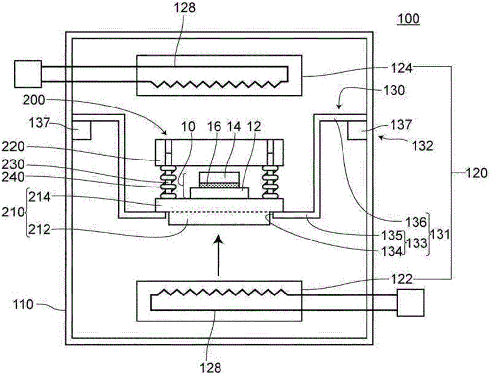
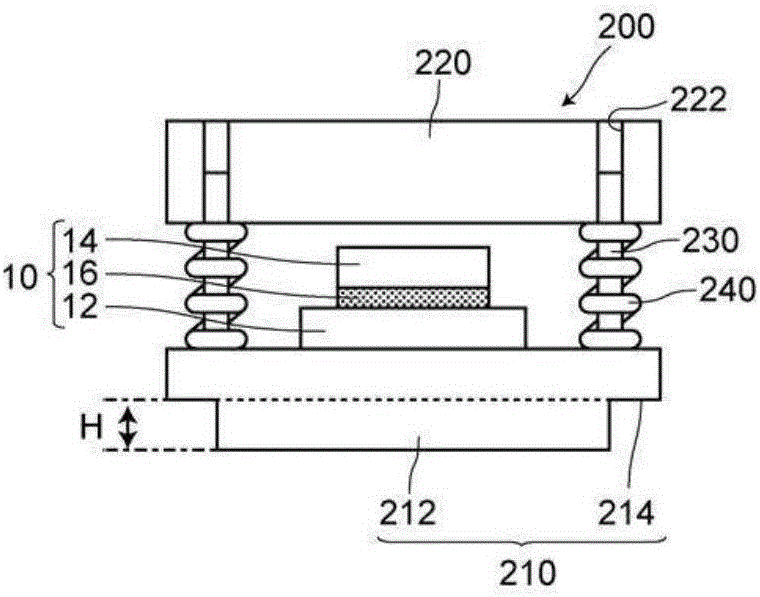
[0042] First, the assembly 10 will be described.

[0043] As shown in FIG. 1, the assembly 10 is an assembly in which electronic components 14 are arranged on a substrate 12 on which a conductor circuit pattern is formed via a metal particle paste 16.

[0044] The "substrate" in this specification refers to a component on which electronic components are mounted.

[0045] The substrate 1 in the first embodiment is, for example, a circuit substrate in which a conductor pattern is formed on a main body made of a non-conductive material. As a constituent material of the substrate 1, a material that can withstand the sintering temperature of the metal particle paste 4 (depending on the type, for example, 300°C) can be used (for example, the body is heat-resistant resin or ceramic, and the wire distribution diagram is Metal).

[0046] In addition, the substrate to which the present invention is applied may be a DCB (Direct Copper Bond) substrate. In addition, the substrate to which the pr...

Embodiment approach 2

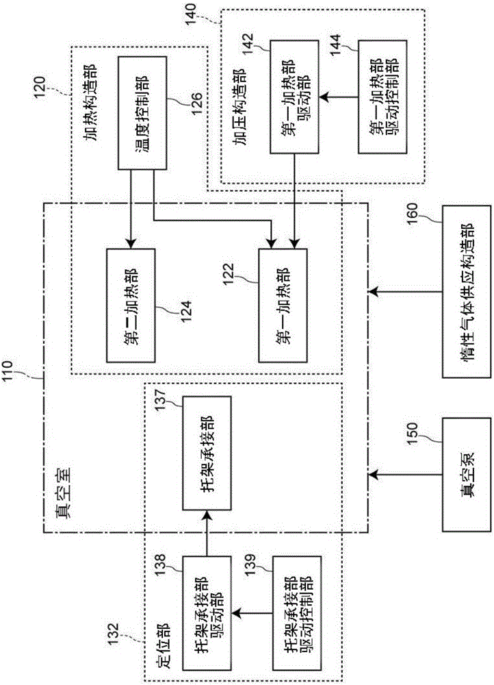
[0113] The bonding device (not shown) according to the second embodiment basically has the same structure as the bonding device 100 according to the first embodiment, but it does not move only the first heating part but also the second heating part. It is different from the joining device 100 related to the first embodiment in one point. That is, in the bonding device according to the second embodiment, the pressurizing structure portion moves the second heating portion downward while moving the first heating portion upward.

[0114] In addition to the components of the pressing structure 140 in the first embodiment, the pressurizing structure unit further includes: a second heating unit driving unit that moves the second heating unit and a second heating unit that controls the second heating unit drive. Department of drive control.


PUM


Abstract

This bonding device 100 is a bonding device that bonds a substrate 12 and an electronic component 14 together by heating, while pressurizing, a pressurization unit 200 including a first transmission member 210 and a second transmission member 220 that sandwich an assembly 10 in which the electronic component 14 is placed on the substrate 12 with a metal particle paste 16 therebetween and that transmit pressure and heat to the assembly, the bonding device comprising: a heating mechanism part 120 including a first heating part 122 and a second heating part 124 that are arranged at positions opposing one another; a positioning mechanism part 130 for positioning the pressurization unit 200 at a position within a space between the first heating part 122 and the second heating part 124 where the pressurization unit contacts neither the first heating part 122 nor the second heating part 124; and a pressurizing mechanism part 140 that pressurizes the pressurization unit 200 by moving the first heating part 122 and / or the second heating part 124. With this bonding device 100, the substrate 12 and the electronic component 14 can be bonded together with high bonding force.

Description

Technical field [0001] The present invention relates to a joining device, a joining method, and a pressing unit. Background technique [0002] In the past, a semiconductor device has been generally recognized and has a structure in which a metal particle paste (Paste) is used to bond a substrate on which a wire pattern is formed and a semiconductor element (for example, refer to Patent Document 1). The metal particle slurry contains nano size or submicron size metal particles in the solvent, and uses the low-temperature sintering phenomenon of metal particles and the low-temperature firing after high surface activity. Conductive paste. [0003] The above-mentioned semiconductor device can be considered to be a substrate and a semiconductor element being bonded using the following bonding device (conventional bonding device 900). The conventional joining device 900 such as Picture 8 Shown is a method of heating and pressing an assembly 10 in which an electronic component 14 (semic...

Claims


Application Information

Patent Timeline
Patent Type & Authority Applications(China)
IPC IPC(8): H01L21/52
CPCH01L21/67092H01L21/67109H01L2224/293H01L2224/75252H01L2224/16145H01L24/75H01L2224/29294H01L2224/75301H01L2224/75251H01L2224/16225H01L2224/75102H01L24/83H01L21/68H01L24/29
Inventor 松林良
Owner SHINDENGEN ELECTRIC MFG CO LTD
Why Eureka
Try Eureka