Stackable MEMS (Micro Electro Mechanical System) sensor package, stackable MEMS sensor chip and preparation method of stackable MEMS sensor chip

A sensor chip and manufacturing method technology, applied in the field of sensors, can solve the problems that restrict the intelligence of MEMS sensors, small size, high cost of MEMS sensors, low sensor performance, etc., to improve the design level and function, reduce process costs, The effect of reducing interference and circuit noise

Active Publication Date: 2017-03-08
XINFOO SENSOR TECH CO LTD
View PDF7 Cites 7 Cited by
  • Summary
  • Abstract
  • Description
  • Claims
  • Application Information

AI Technical Summary

Problems solved by technology

The problems in the existing technology are: 1) The acquisition circuit and the processing circuit are mixed on the same wafer, and the digital and analog circuits will interfere with each other and the noise is large, which is difficult to control, resulting in low performance of the sensor; 2) The acquisition circuit and the processing circuit Mixing on the same wafer will make the size of the electronic component wafer too large, resulting in too large chip area, which is not conducive to application in small-volume scenarios such as hand-held and wearable; 3) The acquisition circuit (analog circuit) can be integrated at the micron level circuit produc

Method used


Image

  • Stackable MEMS (Micro Electro Mechanical System) sensor package, stackable MEMS sensor chip and preparation method of stackable MEMS sensor chip
  • Stackable MEMS (Micro Electro Mechanical System) sensor package, stackable MEMS sensor chip and preparation method of stackable MEMS sensor chip
  • Stackable MEMS (Micro Electro Mechanical System) sensor package, stackable MEMS sensor chip and preparation method of stackable MEMS sensor chip

Examples


Embodiment 1

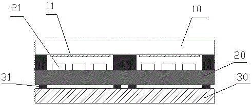
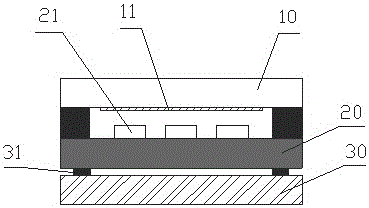
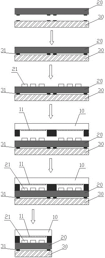
[0041] Embodiment 1: see figure 1 , a stacked MEMS sensor package, comprising: a cover plate 10 for packaging; an acquisition wafer 20, on which an acquisition circuit and a MEMS structure 21 are formed, and the acquisition circuit cooperates with the MEMS structure 21 to realize sensor acquisition signals Function; a processing wafer 30, on which a processing circuit is formed, used to control the acquisition circuit and the MEMS structure 21 to collect signals and process and output the collected signals; the processing wafer 30, the collection wafer 20 and the cover The board 10 is formed by bottom-up bonding using a wafer-level bonding process, wherein a MEMS structure packaging cavity is formed between the cover plate 10 and the collection wafer 20 , and between the collection wafer 20 and the processing wafer 30 Electrical interconnection is realized through conductive bridge piers 31 .

[0042] Further, the lower surface of the cover plate 10 also has a getter material...

Embodiment 2

[0060] Example 2: see Figure 5 , this embodiment also provides a stacked MEMS sensor package, the other parts are the same as in Embodiment 1, the difference is that: the processing wafer 30 is two wafers, which are processing wafer 1 (30a) and processing wafer 1 (30a) respectively. Circle 2 (30b). Preferably, the lower surface of the cover plate 10 also has a getter material layer 11 for realizing a vacuum environment in the packaging cavity, which is suitable for infrared thermal imaging sensors or other MEMS sensors that require vacuum packaging. The conductive bridge piers may be metal piers, or may be made of other materials capable of realizing electrical interconnection. The acquisition circuit adopts 0.13μm~0.5μm integrated circuit technology; the processing circuit adopts 14nm~180nm integrated circuit technology.

[0061] Same as Embodiment 1, the processing circuit on the wafer can include a central processing unit CPU or a microprocessor MPU with control, calcula...

Embodiment 3

[0071] Embodiment 3: see Figure 8, this embodiment also provides a stacked MEMS sensor package, the other parts are the same as in Embodiment 1, the difference is that: the acquisition wafer 20 is two wafers, which are acquisition wafer 1 (20a) and acquisition wafer 1 (20a) respectively. In circle 2 (20b), MEMS structures 21a and 21b are grown on acquisition wafer 1 and acquisition wafer 2, respectively. Here, the functions implemented by the MEMS structures 21a and 21b may be the same or different, and are driven by the acquisition circuit on the acquisition wafer. Preferably, the lower surface of the cover plate 10 also has a getter material layer 11 for realizing a vacuum environment in the packaging cavity, which is suitable for infrared thermal imaging sensors or other MEMS sensors that require vacuum packaging. The conductive bridge piers may be metal piers, or may be made of other materials capable of realizing electrical interconnection. The acquisition circuit adop...


PUM


Abstract

The invention discloses a stackable MEMS (Micro Electro Mechanical System) sensor package, a stackable MEMS sensor chip and a preparation method of the stackable MEMS sensor chip. The package comprises a cover plate, one or more acquisition wafers and one or more processing wafers, wherein the cover plate is used for packaging; acquisition circuits and MEMS structures are formed on the acquisition wafers; processing circuits are formed on the processing wafers; the processing wafers, the acquisition wafers and the cover plate are bonded by a wafer level bonding technology from the bottom up; and all the wafers are electrically connected by conductive bridge piers. According to the package, the chip and the preparation method, the acquisition circuits and the processing circuits are designed in layers, bonding and packaging are performed by the wafer level bonding technology and a vertical multi-layer stackable structure is formed, so that the area of the chip can be significantly reduced; complete isolation of the acquisition circuits and the processing circuits is realized; interference between analog circuits and digital circuits and circuit noise are reduced; a performance index of a sensor is increased; the acquisition circuits and the processing circuits can be separately processed by appropriate technologies, so that the technology cost of the sensor is lowered; and high-performance, small-size and low-cost terminal equipment is applicable.

Description

technical field [0001] The invention relates to the technical field of sensors, in particular to a stacked MEMS sensor package, a chip and a manufacturing method thereof. Background technique [0002] A sensor is a device or device that can sense the measured information and convert it into an electrical signal or other required form of output according to a certain rule. Among a wide variety of sensors, MEMS sensors based on microelectronics and micromachining technologies have become one of the major scientific and technological fields that have attracted worldwide attention. Compared with traditional sensors, it has the characteristics of small size, low cost, low power consumption, easy integration and intelligent realization. At the same time, the feature size of the micron level makes it possible to complete some functions that cannot be realized by traditional mechanical sensors. [0003] The interior of the MEMS sensor mainly includes a MEMS structure for collectin...

Claims


Application Information

Patent Timeline
IPC IPC(8): B81B7/00B81B7/02B81C3/00
CPCB81B7/0009B81B7/02B81C3/001
Inventor 赵照
Owner XINFOO SENSOR TECH CO LTD
Why Eureka
Try Eureka