P type layer-based III nitride enhanced HEMT (High Electron Mobility Transistor) and preparation method thereof

A nitride, p-type layer technology, applied in the field of HEMT device preparation technology, can solve the problems of surface defects, under-etching, p-type layer over-etching, etc., achieve precise control of etching depth, reduce surface damage, The effect of reducing the difficulty of implementation

Pending Publication Date: 2017-03-08
SUZHOU INST OF NANO TECH & NANO BIONICS CHINESE ACEDEMY OF SCI
View PDF5 Cites 10 Cited by
  • Summary
  • Abstract
  • Description
  • Claims
  • Application Information

AI Technical Summary

Problems solved by technology

In the selective etching process, it is necessary to etch a large area of ​​the non-gate area, but if the etching uniformity cannot be effectively controlled, it is very easy to cause over-etching of the p-type layer in the local area, and local There may be under-etching in the region, and both of them will eventually lead to a decrease in the two-dimensional electron gas concentration in the region between the gate source and the gate drain of the device, and generate a large number of surface defect states, which will seriously affect the working of the device. On-resistance and dynamic characteristics when
Therefore, the p-type gate technology based on selective etching requires precise and controllable etching depth of the p-type layer in the non-gate area, which greatly increases the difficulty of the p-type gate technology and makes the repeatability of the technology (piece to piece between), uniformity (between different regions in the chip), and stability (between different rounds of processes) are difficult to guarantee

Method used


Image

  • P type layer-based III nitride enhanced HEMT (High Electron Mobility Transistor) and preparation method thereof
  • P type layer-based III nitride enhanced HEMT (High Electron Mobility Transistor) and preparation method thereof
  • P type layer-based III nitride enhanced HEMT (High Electron Mobility Transistor) and preparation method thereof

Examples


preparation example Construction

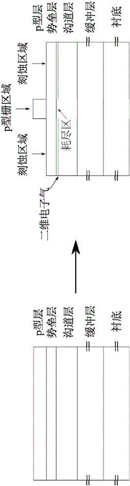
[0062] One aspect of the present invention also provides a method for preparing a group III nitride-enhanced HEMT based on a p-type layer, which includes:

[0063] On the substrate, a first semiconductor layer body as a channel layer, a second semiconductor layer as a barrier layer, and a third semiconductor layer capable of forming a heterojunction with the second semiconductor layer are sequentially grown, wherein, relative to the selected A certain etching substance, the composition material of the region adjacent to the third semiconductor layer in the second semiconductor layer has higher etching resistance than the composition material of the third semiconductor layer,

[0064] Alternatively, the substrate is sequentially grown to form a first semiconductor layer as a channel layer, a second semiconductor layer as a barrier layer, an etching stop layer, and a third semiconductor capable of forming a heterojunction with the second semiconductor layer layer, wherein, relat...

Embodiment 1

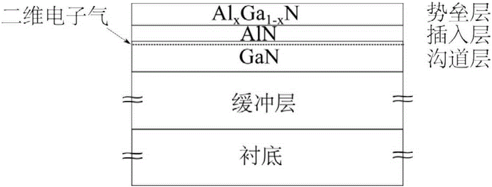
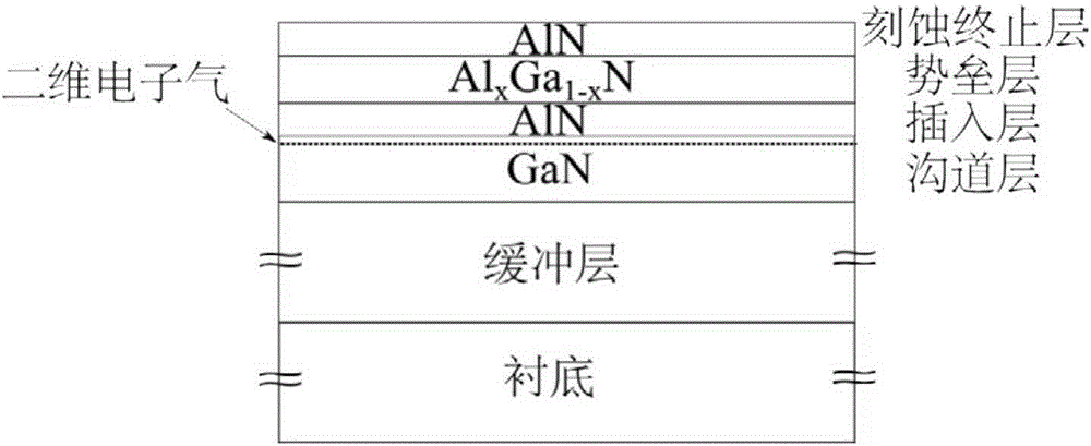
[0075] Embodiment 1 The structure of this HEMT is as Figure 11 As shown, it includes a buffer layer formed on the substrate, Al x Ga 1-x N / GaN heterojunction (x=0.1-0.35), AlN etch stop layer, passivation layer, source electrode (referred to as source), drain electrode (referred to as drain), gate electrode (referred to as gate), etc. Wherein, the substrate may be sapphire, silicon carbide, gallium nitride, aluminum nitride and other substrates, but is not limited thereto. The material of the buffer layer can be commonly used in the industry, for example, GaN, AlGaN, etc. can be used.

[0076] A method for preparing the HEMT provided in this embodiment may include the following steps:

[0077] S1: MOCVD epitaxial growth of HEMT based on AlGaN / GaN heterojunction. Among them, the Al composition x of the AlGaN barrier layer is 10% to 35%, and the thickness is 5 to 25nm; the AlN insertion layer is about 1nm; the GaN channel layer is 50 to 200nm, and the HEMT epitaxial structu...

Embodiment 2

[0087] The structure of embodiment 2 this HEMT is as Figure 14 As shown, it includes a buffer layer formed on the substrate, Al x Ga 1-x N / GaN heterojunction (x=0.1-0.4), passivation layer, source electrode (referred to as source), drain electrode (referred to as drain), gate electrode (referred to as gate), etc. In the barrier layer, the Al composition changes stepwise with the growth z direction, and the high Al composition AlGaN acts as the etch stop layer (Al 0.4 Ga 0.6 N).

[0088] A method for preparing the HEMT provided in this embodiment may include the following steps:

[0089] S1: MOCVD epitaxial growth of HEMT based on AlGaN / GaN heterojunction. Among them, the Al composition x of the AlGaN barrier layer is 10%, 20%, 30%, and 40% along the epitaxial growth z direction, and the thickness of the barrier layer is 5-25nm; the AlN insertion layer is about 1nm; the GaN channel layer is 50~200nm, HEMT epitaxial structure such as Figure 12a-Figure 12b shown.

[009...


PUM


Abstract

The invention discloses a p type layer-based III nitride enhanced HEMT (High Electron Mobility Transistor) and a preparation method thereof. The HEMT comprises a heterojunction mainly formed by a first semiconductor layer and a second semiconductor layer, and a source electrode, a gate electrode and a drain electrode connected with the heterojunction; a third semiconductor layer capable of forming a heterojunction with the second semiconductor layer is also distributed between the gate electrode and a barrier layer; an etching stop layer is also distributed between the third semiconductor layer and the second semiconductor layer; the composition material of the etching stop layer has a higher etching selectivity ratio than that of the third semiconductor layer, or, the composition material of an area, close to the third semiconductor layer, in the second semiconductor layer has a higher etching selectivity ratio than that of the third semiconductor layer. Due to the design of the invention, the p type gate technology implementation difficulty can be greatly reduced, the p type layer etching depth can be precisely controlled, electrical features of the device and the repeatability, the uniformity, and the stability of a chip manufacturing process are ensured, and mass production is facilitated.

Description

technical field [0001] The invention relates to a preparation process of a HEMT device, in particular to a preparation method of a Group III nitride enhanced HEMT using an etching stop layer. Background technique [0002] Compared with traditional silicon-based MOSFETs, high electron mobility transistors (High Electron Mobility Transistors, HEMTs) based on AGaN / GaN heterojunctions have the advantages of low on-resistance, high breakdown voltage, and high switching frequency, so they can be used in various It is used as a core device in similar power conversion systems, and has important application prospects in energy saving and consumption reduction. However, due to the polarization effect of the III-nitride material system, generally speaking, HEMTs based on AlGaN / GaN heterojunctions are depletion mode (normally on). When this type of device is applied to a circuit-level system, it needs Designing a negative polarity gate drive circuit to realize switching control of the ...

Claims


Application Information

Patent Timeline
Patent Type & Authority Applications(China)
IPC IPC(8): H01L21/335H01L29/778H01L21/02H01L21/3065
CPCH01L21/0254H01L21/3065H01L29/66462H01L29/7783
Inventor 孙钱周宇李水明陈小雪戴淑君高宏伟冯美鑫杨辉
Owner SUZHOU INST OF NANO TECH & NANO BIONICS CHINESE ACEDEMY OF SCI
Why Eureka
Try Eureka