Display substrate and driving method thereof and display device

A technology for displaying substrates and display areas, which is applied in the direction of instruments, semiconductor devices, circuits, etc., and can solve problems such as increased thickness of display devices

Active Publication Date: 2017-03-15
BOE TECH GRP CO LTD +1
View PDF6 Cites 3 Cited by
  • Summary
  • Abstract
  • Description
  • Claims
  • Application Information

AI Technical Summary

Problems solved by technology

[0004] Embodiments of the present invention provide a display substrate, a driving method thereof, and a display

Method used


Image

  • Display substrate and driving method thereof and display device
  • Display substrate and driving method thereof and display device
  • Display substrate and driving method thereof and display device

Examples


Embodiment 1

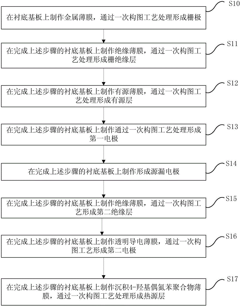
[0048] Embodiment 1. In this embodiment, the array substrate includes a plurality of sub-pixels arranged in a matrix. In this case, the position of the heat source layer 12 corresponds to the light-transmitting area of ​​the sub-pixel, and the pattern of the heat source layer 12 is consistent with the shape of the light-transmitting area. The following is the preparation method of the array substrate, such as image 3 Shown include:

[0049] Step S10, such as Figure 4a As shown, the gate 102 is formed on the base substrate 101 through a patterning process.

[0050] Specifically, a metal thin film may be prepared on the base substrate 101 first. The gate 102 is then formed through a patterning process. Wherein, the gate 102 is made of a metal material, and the metal material can generally be metals such as molybdenum, aluminum, aluminum-nickel alloy, molybdenum-tungsten alloy, chromium, or copper, or a combination structure of the above-mentioned thin films.

[0051] It s...

Embodiment 2

[0069] Embodiment 2 In this embodiment, when the display substrate 01 is an array substrate, the pattern of the heat source layer 12 is consistent with the shape of the display area 10 of the display substrate 01 . The preparation method of the array substrate is as follows, including:

[0070] Such as Figure 8a As shown, the preparation method of forming the gate 102, the first insulating layer 103, the active layer 104, the pixel electrode 105, the source and drain electrodes 106, the second insulating layer 107, and the common electrode 108 on the base substrate 101 in sequence is the same as the above step S10 - The step S16 is the same and will not be repeated here. The difference is: on the base substrate 101 formed with the common electrode 108, a patterning process such as Figure 8a The heat source layer 12 is shown.

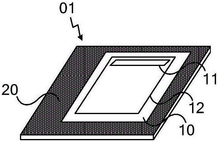
[0071] In this embodiment, the heat source layer 12 is located in the display area 10 and conforms to the shape of the display area 10 . Since the...


PUM


Abstract

The embodiment of the invention provides a display substrate and a driving method thereof and a display device and relates to the technical field of display. The display substrate is used for solving the problem of increase of the thickness of a display device caused by a heating plate. The display substrate comprises a display area and a non-display area. The display substrate further comprises a trigger electrode arranged on the display area and a heat source layer. The trigger electrode is in contact with the heat source layer and is used for receiving thermal pulse signals and performing thermal trigger on the heat source layer. The heat source layer is used for absorbing light energy, performing photothermal conversion under thermal trigger of the trigger electrode, and converting the stored light energy into thermal energy for release. The display substrate is used for manufacturing the display device.

Description

technical field [0001] The present invention relates to the field of display technology, in particular to a display substrate, a driving method thereof, and a display device. Background technique [0002] Liquid crystal display devices are mainly composed of array substrates, color filter substrates and liquid crystals. Due to their small size, low power consumption, no radiation, and relatively low production costs, liquid crystal display devices have been widely used in various fields. In practical applications, liquid crystal display devices sometimes need to be used in low-temperature environments, such as low-temperature environments in high-altitude and high-latitude regions. However, in a low temperature environment, the viscosity coefficient of the liquid crystal in the liquid crystal display device will increase, so that the rotation speed of the liquid crystal will slow down, and then the response time of the liquid crystal display device will become longer and the...

Claims


Application Information

Patent Timeline
IPC IPC(8): G02F1/1333H01L23/34
CPCG02F1/133382H01L23/345
Inventor 王杨刘庭良高山郭威李挺向西徐元杰臧鹏程
Owner BOE TECH GRP CO LTD
Why Eureka
Try Eureka