
Preparation method of semiconductor device

A semiconductor and device technology, applied in the field of semiconductor device preparation, can solve problems such as short circuit between gate and polysilicon layer, uncontrollable distance between polysilicon layers, etc., and achieve the effect of reducing width, avoiding short circuit, and improving process accuracy

Active Publication Date: 2019-07-23
SEMICON MFG INT TIANJIN +1
View PDF3 Cites 0 Cited by
  • Summary
  • Abstract
  • Description
  • Claims
  • Application Information

AI Technical Summary

Problems solved by technology

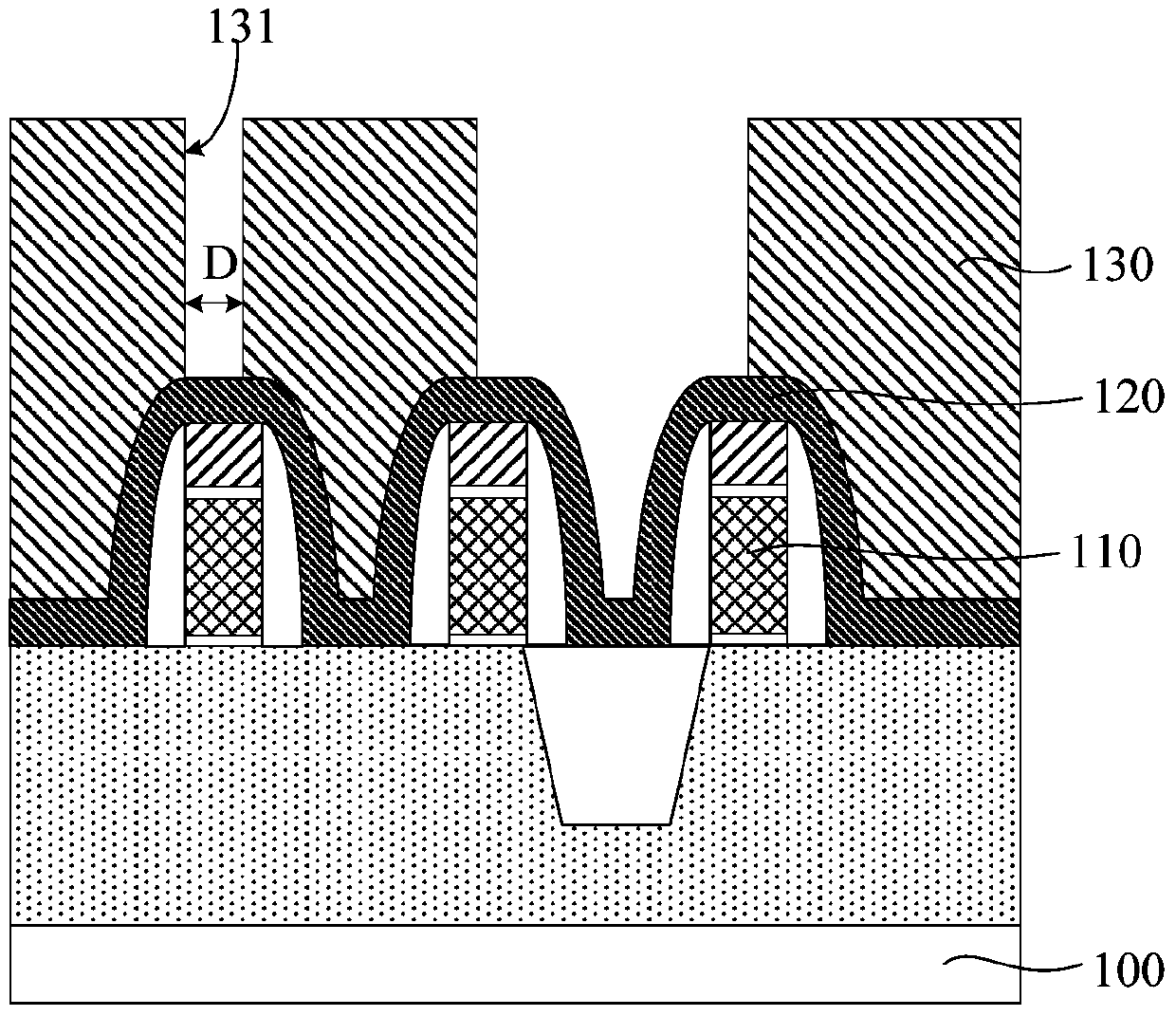
However, with the reduction of the size of the SRAM, the width D of the opening 131 needs to be about 30nm. The existing photolithography process has been difficult to meet the requirement of the opening width, so that the distance between the polysilicon layers cannot be controlled. Defects that cause short circuits between gates and polysilicon layers in existing SRAMs

Method used


Image

  • Preparation method of semiconductor device
  • Preparation method of semiconductor device
  • Preparation method of semiconductor device

Examples


preparation example Construction

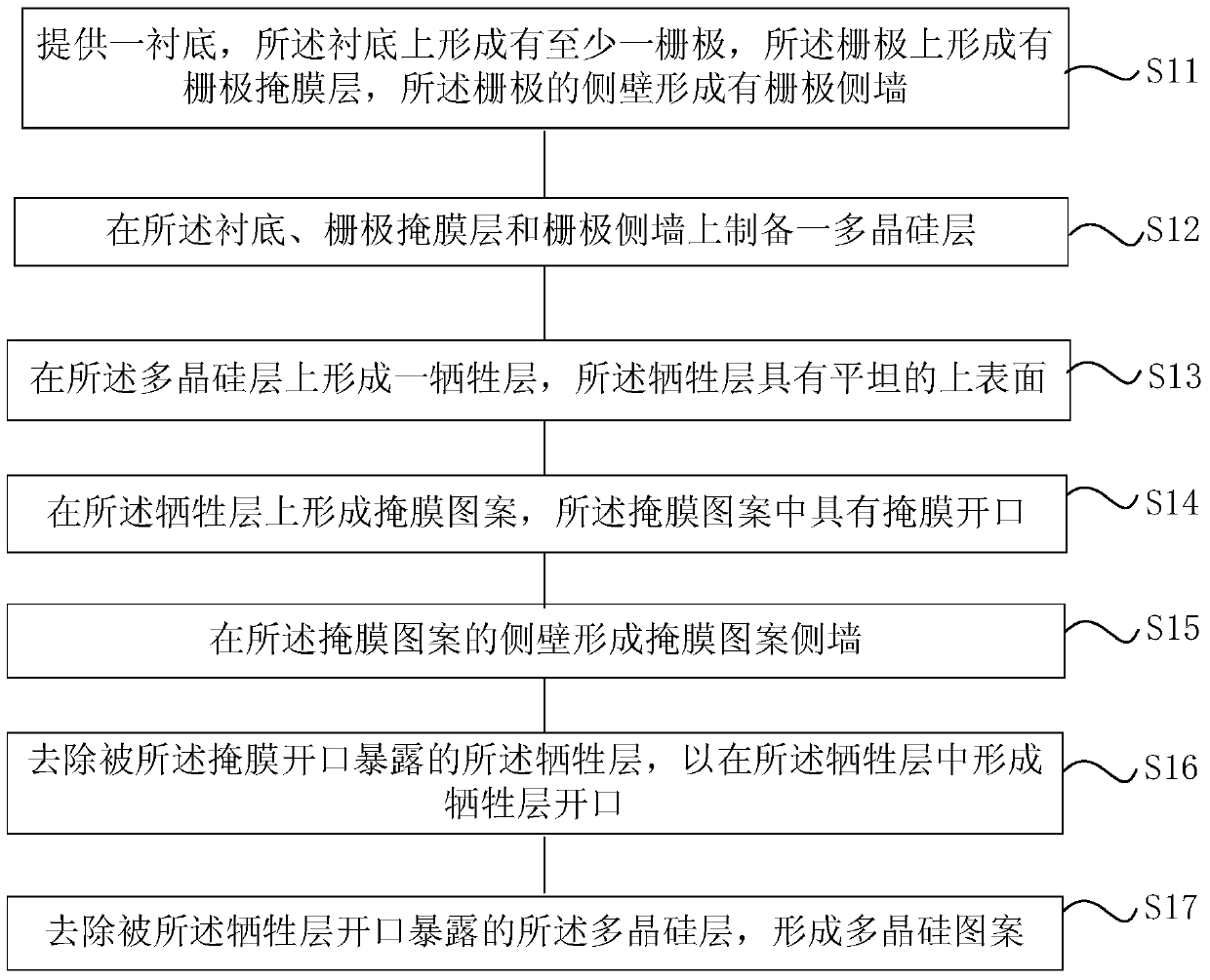
[0040] The core idea of ​​the present invention is to provide a method for preparing a semiconductor device, such as figure 2 shown, including:

[0041] Step S11: providing a substrate, on which at least one gate is formed, a gate mask layer is formed on the gate, and gate sidewalls are formed on the side walls of the gate;

[0042] Step S12: preparing a polysilicon layer on the substrate, the gate mask layer and the gate sidewall;

[0043] Step S13: forming a sacrificial layer on the polysilicon layer, the sacrificial layer having a flat upper surface;

[0044] Step S14: forming a mask pattern on the sacrificial layer, the mask pattern having a mask opening;

[0045] Step S15: forming sidewalls of the mask pattern on the sidewalls of the mask pattern;

[0046] Step S16: removing the sacrificial layer exposed by the mask opening to form a sacrificial layer opening in the sacrificial layer; and

[0047] Step S17: removing the polysilicon layer exposed by the sacrificial la...

no. 1 example

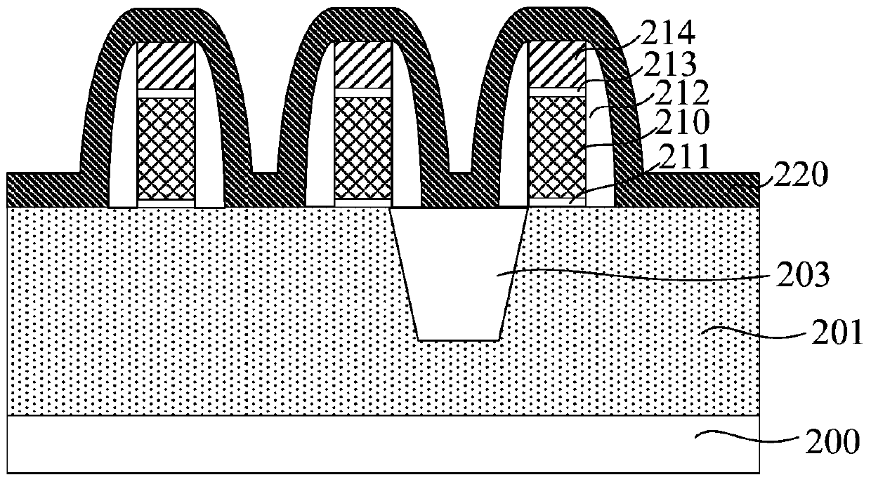
[0051] see Figure 3-Figure 11 The first embodiment of the present invention is specifically described, wherein, Figure 3-Figure 11 It is a schematic diagram of the structure of the semiconductor device in the first embodiment of the present invention during the manufacturing process.

[0052] First, if image 3As shown, step S11 is performed to provide a substrate 200, on which at least one gate 210 is formed, a gate mask layer 214 is formed on the gate 210, and the sidewall of the gate 210 A gate spacer 212 is formed. The substrate 200 includes a well region 201 , and an isolation region 203 is also disposed in the substrate 200 , which is common knowledge in the art and will not be described in detail here. exist image 3 Three gates 210 are shown in , and in other embodiments of the present invention, 2, 4, 5 or more gates 210 may also be disposed on the substrate 200 . In this embodiment, a gate oxide layer 211 may be provided between the substrate 200 and the gate ...

no. 2 example

[0065] see Figure 12-Figure 18 ,in, Figure 12-Figure 18 It is a schematic diagram of the structure of the semiconductor device in the second embodiment of the present invention during the manufacturing process. exist Figure 12-Figure 8 , the reference numerals indicate the same Figure 3-Figure 11 The same expression is the same structure as the first embodiment. The manufacturing method of the semiconductor device of the second embodiment is basically the same as the manufacturing method of the semiconductor device, the difference is that: the material of the sacrificial layer is the same as that of the gate mask layer, and the specific preparation steps are as follows :

[0066] Such as Figure 12 As shown, in the step S11, the material of the gate mask layer 314 is oxide, and the material of the gate spacer 312 is nitride.

[0067] Then go to step S12 and continue to refer to Figure 12 , preparing a polysilicon layer 220 on the substrate 200 , the gate mask layer...


PUM


Abstract

The invention discloses a manufacturing method of a semiconductor device, comprising: providing a substrate, at least one gate is formed on the substrate, a gate mask layer is formed on the gate, and the side of the gate A gate sidewall is formed on the wall; a polysilicon layer is prepared on the substrate, the gate mask layer and the gate sidewall; a sacrificial layer is formed on the polysilicon layer, and the sacrificial layer has a flat upper surface ; forming a mask pattern on the sacrificial layer, with a mask opening in the mask pattern; forming a mask pattern side wall on the side wall of the mask pattern; removing the mask pattern exposed by the mask opening a sacrificial layer to form a sacrificial layer opening in the sacrificial layer; and removing the polysilicon layer exposed by the sacrificial layer opening to form a polysilicon pattern. The preparation method of the semiconductor device provided by the invention can effectively improve the reliability of the SRAM.

Description

technical field [0001] The invention relates to the technical field of semiconductor manufacturing, in particular to a method for preparing a semiconductor device. Background technique [0002] With the continuous development of modern high-tech industries represented by electronic communication technology, the total output value of the world's integrated circuit industry is growing at a rate of more than 30% per year. As an important storage device, static random access memory (SRAM) is widely used in digital and communication circuit design. SRAM is an important component in logic circuits, and it is widely used in data storage because of its advantages of low power consumption and high reading speed. [0003] With the miniaturization of memory cells and the high integration requirements of semiconductor devices, the size of the SRAM is getting smaller and smaller. However, the critical dimensions of the active area in the SRAM, the critical dimensions of the gate, and th...

Claims


Application Information

Patent Timeline
Patent Type & Authority Patents(China)
IPC IPC(8): H01L21/8244
CPCH10B10/00
Inventor 李敏吴永玉
Owner SEMICON MFG INT TIANJIN
Learn More