Gate voltage bootstrap switch circuit

A switch circuit and grid voltage bootstrap technology, which is applied in the field of grid voltage bootstrap switch circuits, can solve the problems of lower main switch tube grid terminal voltage, deterioration of switch circuit linearity, bootstrap capacitor charge loss, etc., to reduce the circuit area , easy to implement and apply, eliminates the effect of charge sharing

Active Publication Date: 2017-03-15
UNIV OF ELECTRONICS SCI & TECH OF CHINA
View PDF5 Cites 3 Cited by
  • Summary
  • Abstract
  • Description
  • Claims
  • Application Information

AI Technical Summary

Problems solved by technology

[0011] However, when the phase is turned on, the MOS transistor (M 1 ~ M 5 ) of parasitic capacitance (C GS 、C GD 、C SB 、C DB etc.) with the bootstrap capacitor C 1 Charge sharing will occur, resulting in the loss of charge on the bootstrap capacitor, reducing the voltage at the gate terminal of the main switch, thereby reducing the on-resistance; at the same time, the capacitance of the above-mentioned parasitic capacitor is directly related to the input voltage, which will further deteriorate the linearity of the switching circuit
In order to reduce the influence of parasitic capacitance, the traditional bootstrap switch circuit is usually implemented by increasing the bootstrap capacitance, but this will increase the chip area and increase the cost

Method used


Image

  • Gate voltage bootstrap switch circuit
  • Gate voltage bootstrap switch circuit
  • Gate voltage bootstrap switch circuit

Examples


Embodiment Construction

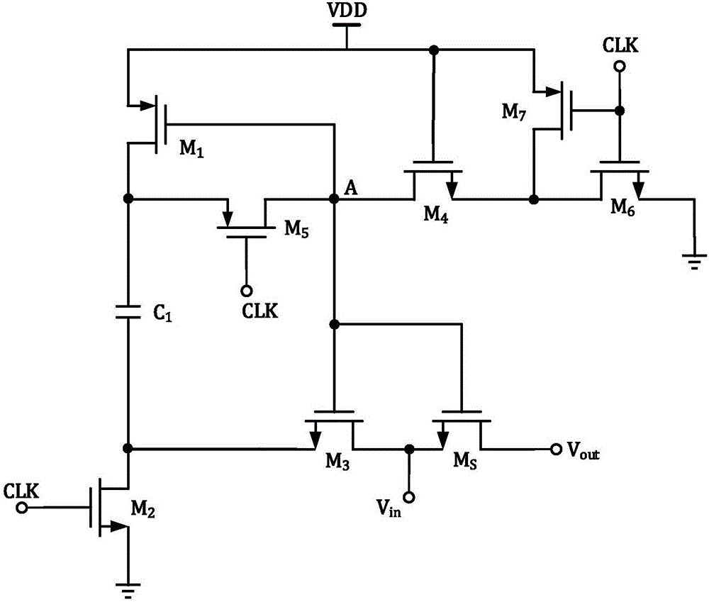
[0034] The technical scheme of the present invention will be described in detail below in conjunction with the accompanying drawings and embodiments.

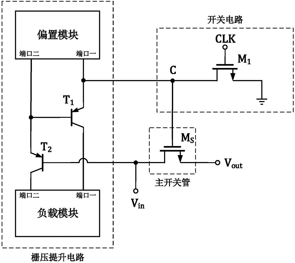
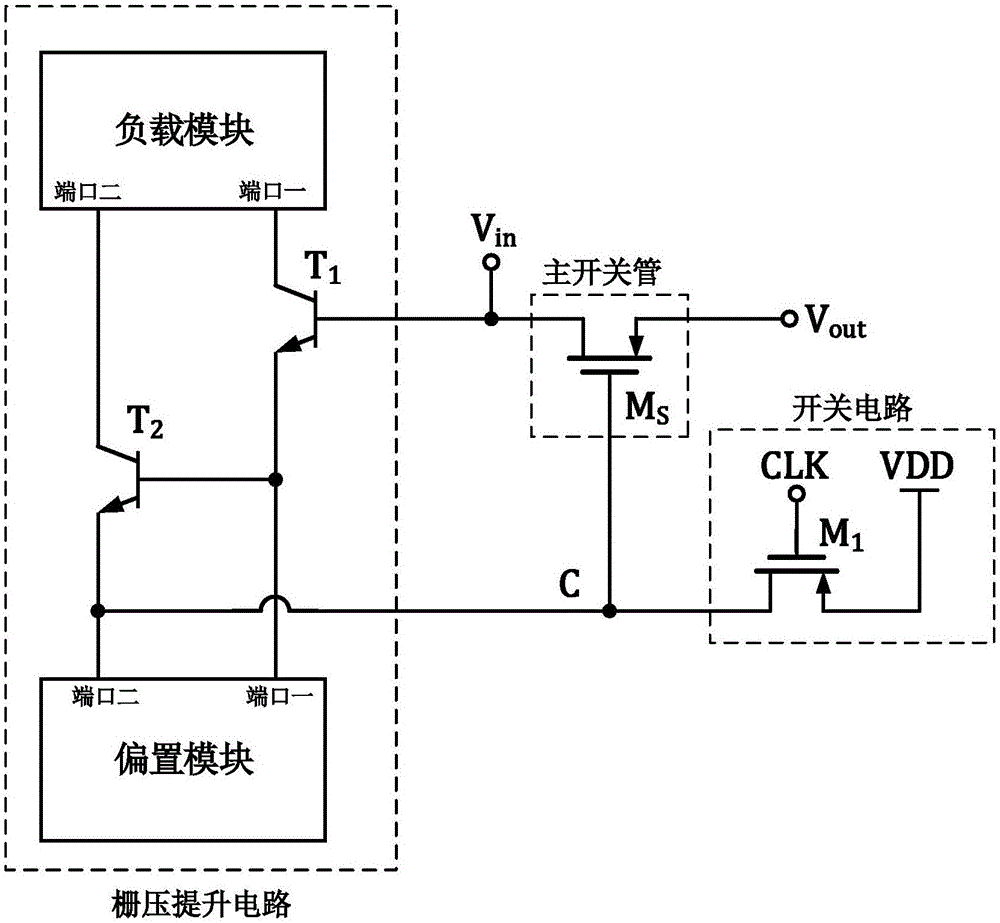
[0035] Such as figure 2 As shown, a gate voltage bootstrap switching circuit provided by the present invention includes a main switching tube M s , gate voltage boost circuit, switch circuit, input signal V in , output signal V out ;

[0036] The main switch M s is an NMOS transistor whose drain is connected to the input signal V in , the source is connected to the output signal V out , the gate is connected to node C;

[0037] The grid voltage boosting circuit includes a bias module, a load module and two transistors T connected in an emitter-follower manner 1 and T 2 , the bias module is a dual-port module, used to provide current bias to the branch, and the load module is a dual-port module, used to provide load to the branch; the two are connected in the form of an emitter follower The triode T 1 and T 2 It is a...


PUM


Abstract

A gate voltage bootstrap switch circuit belongs to the simulation integration circuit design field. The circuit comprises a main switch tube Ms, a gate voltage boost circuit, a switch circuit, an input signal Vin and an output signal Vout. The gate voltage boost circuit comprises a bias module, a load module and two triodes which are connected in an emitter follower mode and is used for changing a gate end voltage of the main switch tube so as to realize that a gate source voltage is a constant value. The switch circuit is a transistor and is used for controlling opening and closing of the gate voltage boost circuit. The input signal Vin is connected to a gate end of the main switch tube Ms through the two triodes which are connected in the emitter follower mode in the gate voltage boost circuit. A source end of the main switch tube Ms is connected to the output signal Vout. The invention provides the gate voltage bootstrap switch circuit without a bootstrap capacitor, a charge sharing problem brought by a parasitic capacitor is eliminated and a circuit area is effectively reduced.

Description

technical field [0001] The invention belongs to the field of analog integrated circuit design, in particular to a gate voltage bootstrap switch circuit. Background technique [0002] With the rapid development of modern communication technology and signal processing technology, the demand for high-speed, high-precision semiconductor integrated circuits is increasing. In the field of signal processing, it is necessary to convert the analog signal into a digital signal, and then carry out further processing through the digital signal processing module. In the process of converting an analog signal to a digital signal, in order to meet the requirement for high linearity sampling of the analog signal, a grid voltage bootstrap switch circuit is usually required. [0003] The traditional gate voltage bootstrap switch circuit structure such as figure 1 As shown, by the main switch tube M s and a gate voltage bootstrap circuit, where the gate voltage bootstrap circuit includes a ...

Claims


Application Information

Patent Timeline
Patent Type & Authority Applications(China)
IPC IPC(8): H03K17/00
CPCH03K17/00
Inventor 李靖徐成阳吴辉贵王明辉宁宁于奇
Owner UNIV OF ELECTRONICS SCI & TECH OF CHINA
Why Eureka
Try Eureka