Image automatic recognition system based on wafer internal defect detection

An automatic identification system and defect technology, applied in image enhancement, image analysis, image data processing and other directions, can solve the problems of increasing the workload of engineers, prone to errors, and increasing the workload of engineers, avoiding machine pollution and reducing manpower. cost, the effect of reducing unnecessary losses

Inactive Publication Date: 2017-03-22
WUHAN XINXIN SEMICON MFG CO LTD
View PDF4 Cites 13 Cited by
  • Summary
  • Abstract
  • Description
  • Claims
  • Application Information

AI Technical Summary

Problems solved by technology

[0003] Relying on the human eye to judge defects not only increases the engineer's workload (load), but also is prone to errors; because the grayscale and bubbles of the wafer cannot be quantified, the engineer is not only unable to obtain the gray edge and bubble defects generated during the wafer manufacturing process In addition, it is impossible to obtain the abnormality of the machine during the wafer manufacturing process; at the same time, relying on the manual production of defect trend charts (bubble charts) not only increases the workload of engineers, but also cannot find the abnormality of the process or machine in a timely and effective manner. , which is not expected by those skilled in the art

Method used


Image

  • Image automatic recognition system based on wafer internal defect detection
  • Image automatic recognition system based on wafer internal defect detection

Examples


Embodiment Construction

[0025] The present invention will be further described below in conjunction with the accompanying drawings and specific embodiments, but not as a limitation of the present invention.

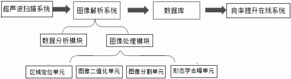
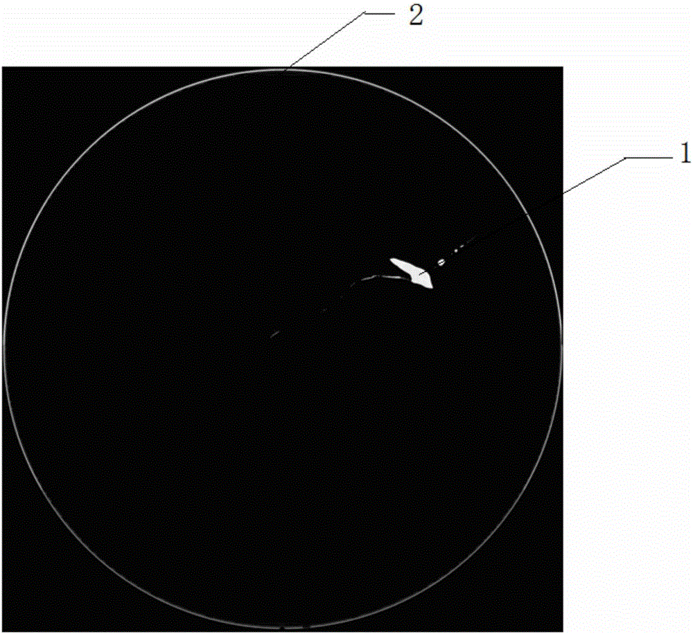
[0026] Such as figure 1 As shown, this embodiment relates to an image automatic recognition system based on wafer internal defect detection. Specifically, the image recognition system includes an ultrasonic scanning system, an image analysis system, a database, and an online system for improving yield; Scan to obtain the original image of the wafer, the original image of the wafer obtained by the ultrasonic scanning system is as follows figure 2 As shown; the image analysis system is connected with the ultrasonic scanning system, and the image analysis system includes an image segmentation unit and a morphological denoising unit to analyze and process the original image by using an image morphological algorithm to obtain wafer defect information; the database and The image analysis system is c...


PUM


Abstract

The invention relates to the technical field of semiconductor manufacturing and especially relates to an image automatic recognition system based on wafer internal defect detection. On the basis of data analysis, an image analysis system comprising image segmentation and morphological denoising is used, the original image obtained by the ultrasonic scanning of a wafer is analysis, the information of positions and sizes of a grey edge and a bubble defect in the wafer is obtained, then the information is stored into a corresponding database, through calling the corresponding information, a defect sketch map and a trend chart which satisfies a client requirement is automatically generated, thus the abnormality in the wafer process and the abnormality of a machine platform are effectively and timely found, the labor cost is reduced, the pollution of the machine is avoided, and thereby the unnecessary loss is reduced.

Description

technical field [0001] The invention relates to the technical field of semiconductors, in particular to an image automatic recognition system based on wafer internal defect detection. Background technique [0002] From the beginning of CIS (CIS: Color Image Sensor color image sensor) products, during the manufacturing process, wafers continue to produce (suffer) gray edge (chipping) and bubble (bubble) defects (defect). In the subsequent process of the wafer, due to gray edge defects, defects such as wafer skin peeling and copper precipitation may occur, directly polluting the machine. If the bubble defect is damaged, it may directly cause copper precipitation, scratches and other defects, directly pollute the machine, and in severe cases, the wafer will be scrapped directly, wasting a lot of resources. These abnormalities are caused by abnormalities in the manufacturing process or machines. If they cannot be detected in a timely and effective manner, a large wave of wafers...

Claims


Application Information

Patent Timeline
Patent Type & Authority Applications(China)
IPC IPC(8): G06T7/00G06F17/30H01L21/66
CPCG06T7/0004G06F16/248G06T2207/10132G06T2207/30148H01L22/12
Inventor 罗聪严诗佳
Owner WUHAN XINXIN SEMICON MFG CO LTD
Why Eureka
Try Eureka