Double-junction single-photon avalanche diode and its fabrication method
A single-photon avalanche and diode technology, applied in the field of single-photon detection, can solve problems such as low photon detection efficiency, achieve high photon detection efficiency, improve absorption rate, and increase the effect of avalanche multiplication area
- Summary
- Abstract
- Description
- Claims
- Application Information
AI Technical Summary
Problems solved by technology
Method used
Image
Examples
Embodiment Construction
[0018] The present invention will be further described below in conjunction with the accompanying drawings.
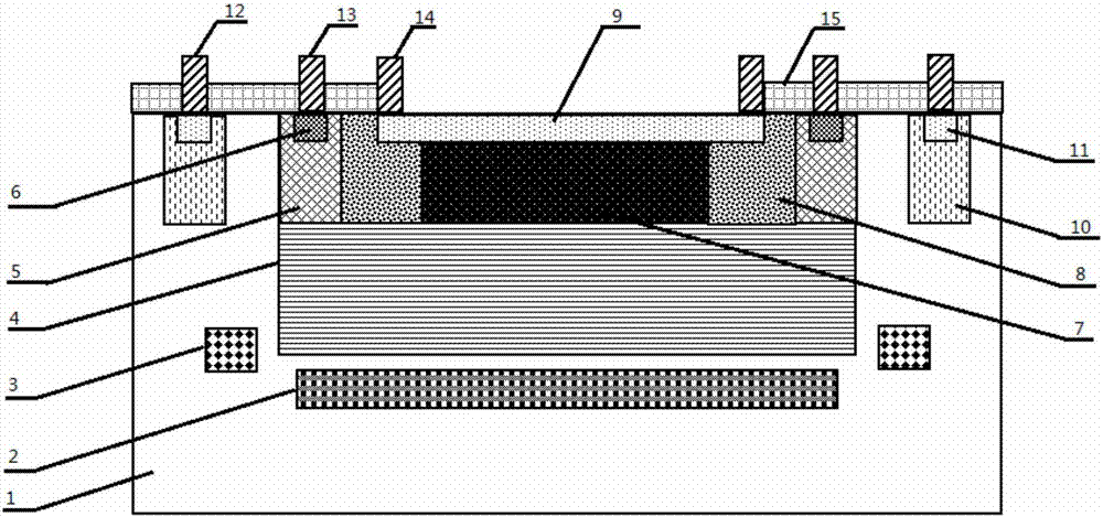
[0019] refer to figure 1 , a double-junction single-photon avalanche diode, including a cylindrical p-substrate layer 1, a p-well charge layer 2, an inversion deep n-well 4, an n-well charge layer 7, and a p+-type light absorption layer 9, and an annular p doping control region 3, n well layer 5, n+ type semiconductor layer 6, p-type semiconductor layer 8, p well layer 10, p+ type semiconductor layer 11, GND electrode 12, cathode electrode 13, anode electrode 14 and two Silicon oxide layer 15; p-substrate layer 1, p well charge layer 2, p doping control region 3, inversion deep n well 4, n well layer 5, n+ type semiconductor layer 6, n well charge layer 7, p- Type semiconductor layer 8, p+ type light absorbing layer 9, p well layer 10, p+ type semiconductor layer 11, GND electrode 12, cathode electrode 13, anode electrode 14 and silicon dioxide layer 15 are all arrang...
PUM
 Abstract
Description
Claims
Application Information
 - R&D Engineer
- R&D Manager
- IP Professional
- Industry Leading Data Capabilities
- Powerful AI technology
- Patent DNA Extraction
Browse by: Latest US Patents, China's latest patents, Technical Efficacy Thesaurus, Application Domain, Technology Topic, Popular Technical Reports.
© 2024 PatSnap. All rights reserved.Legal|Privacy policy|Modern Slavery Act Transparency Statement|Sitemap|About US| Contact US: help@patsnap.com


