Method of wafer scale fabrication and assembly of a liquid crystal electro-optic device

An electro-optical device, liquid crystal technology, applied in chemical instruments and methods, optics, liquid crystal materials, etc., can solve problems such as pollution

Active Publication Date: 2017-03-22
LENSVECTOR
View PDF9 Cites 5 Cited by
  • Summary
  • Abstract
  • Description
  • Claims
  • Application Information

AI Technical Summary

Problems solved by technology

[0006] In view of the above state of the art, there is a need to develop another approach to wafer-level fabricated LCL optical devices to allow simpler assembly and address contamination issues

Method used


Image

  • Method of wafer scale fabrication and assembly of a liquid crystal electro-optic device
  • Method of wafer scale fabrication and assembly of a liquid crystal electro-optic device
  • Method of wafer scale fabrication and assembly of a liquid crystal electro-optic device

Examples


Embodiment Construction

[0030] The above problems can be solved according to the proposed solution, where:

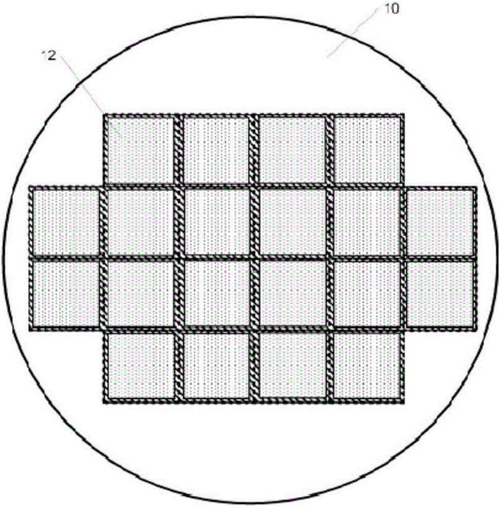
[0031] The fabrication of LCL optics is delicate and, in particular, more complex than fabrication of conventional all-solid-state integrated circuits. Referring to Fig. 1, an LCL wafer 10 is a 2D array of several thousand LCL optical devices 12, which, due to the liquid nature of the LC layer(s) employed, must contain a large number of liquid reservoirs. In the context of this patent application, "wafer" may refer to a substrate of any shape (eg round, rectangular, etc.) and of any type (eg glass, silicon, sapphire).

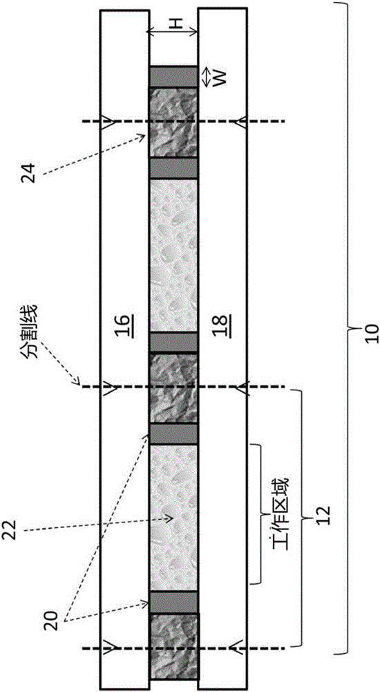
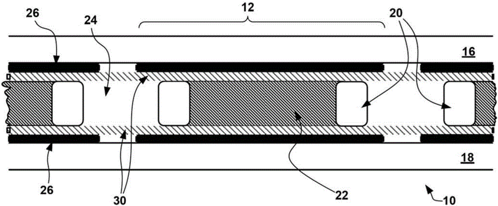
[0032] For simplicity of illustration, the LC material is birefringent and the figures show polarization-dependent LCL optics (one layer of LC on a single wafer). For example, referring to FIG. 2, each final (cut from wafer) LCL optical device 12 includes a substrate 16, 18, and an LC reservoir 22 containing a working fluid separated by a (viscous) reservoir wall 20 which can ...


PUM


Abstract

A method of wafer level manufacturing and assembly of a liquid crystal optical device is disclosed. An electro-optic device having at least one liquid crystal cell for providing spatially variable control of light is also described. The electro-optic device includes: a pair of opposed substrates sandwiching a liquid crystal layer therebetween; a pair of electrodes for applying an electric field therebetween, each electrode being deposited on a corresponding substrate; and a liquid crystal reservoir wall defining a lateral extent of the liquid crystal layer between the substrates. The reservoir wall includes: a first bottom barrier deposited on a bottom one of the pair of substrates; and a second curable top barrier deposited on the top substrate outside the first barrier. The first barrier and second uncured barrier are configured to merge on contact to retain liquid crystal material inside the reservoir wall prior to curing the second barrier.

Description

[0001] This application claims priority to US Provisional Application No. 61 / 988,522, filed May 5, 2014. technical field [0002] The present invention relates to liquid crystal electro-optic devices, in particular to the manufacture and wafer-level assembly of liquid crystal electro-optical devices. Background technique [0003] Wafer-level manufacturing processes are used in technologies such as manufacturing integrated circuits, image sensors, microlens arrays, etc. This parallel wafer-level fabrication uses limited processing steps to obtain thousands of such devices simultaneously, thereby reducing their manufacturing costs. However, fabrication and assembly of arrays for wafer-scale fabricated liquid crystal lens devices still has some of the most challenging processing steps. A method that must be specially tuned for each specific manufacturing process. [0004] Electrically controllable (tunable), gradient index, liquid crystal lenses (TLCLs) are well known in the ...

Claims


Application Information

Patent Timeline
Patent Type & Authority Applications(China)
IPC IPC(8): G02F1/1333C09K19/02
CPCG02F1/1333G02F1/133377G02F1/1337G02F1/133351G02F1/13394G02F1/1341G02F1/134309G02F1/13439G02F1/13415
Inventor 迪格兰·加尔斯蒂安阿拉姆·巴格拉姆亚恩阿米尔·图尔克大卫·尹谢尔盖·雅科文科
Owner LENSVECTOR
Why Eureka
Try Eureka