
Differential power analysis defense adder employing sense amplifier based logic

A differential power analysis and adder technology, applied in the field of adders, can solve problems such as increased energy consumption, complex timing control, and complex interface circuit design

Active Publication Date: 2017-03-29
NINGBO UNIV
View PDF3 Cites 9 Cited by
  • Summary
  • Abstract
  • Description
  • Claims
  • Application Information

AI Technical Summary

Problems solved by technology

Compared with SABL, TDPL balances power consumption by introducing an additional discharge stage, which increases its energy consumption. If the attacker modifies the clock to generate a separate discharge stage power consumption, the TDPL anti-DPA attack performance will be greatly reduced; ADDL timing control is complex, and When interacting with CMOS circuits, complex interface circuits need to be designed

Method used


Image

  • Differential power analysis defense adder employing sense amplifier based logic
  • Differential power analysis defense adder employing sense amplifier based logic
  • Differential power analysis defense adder employing sense amplifier based logic

Examples


Embodiment 1

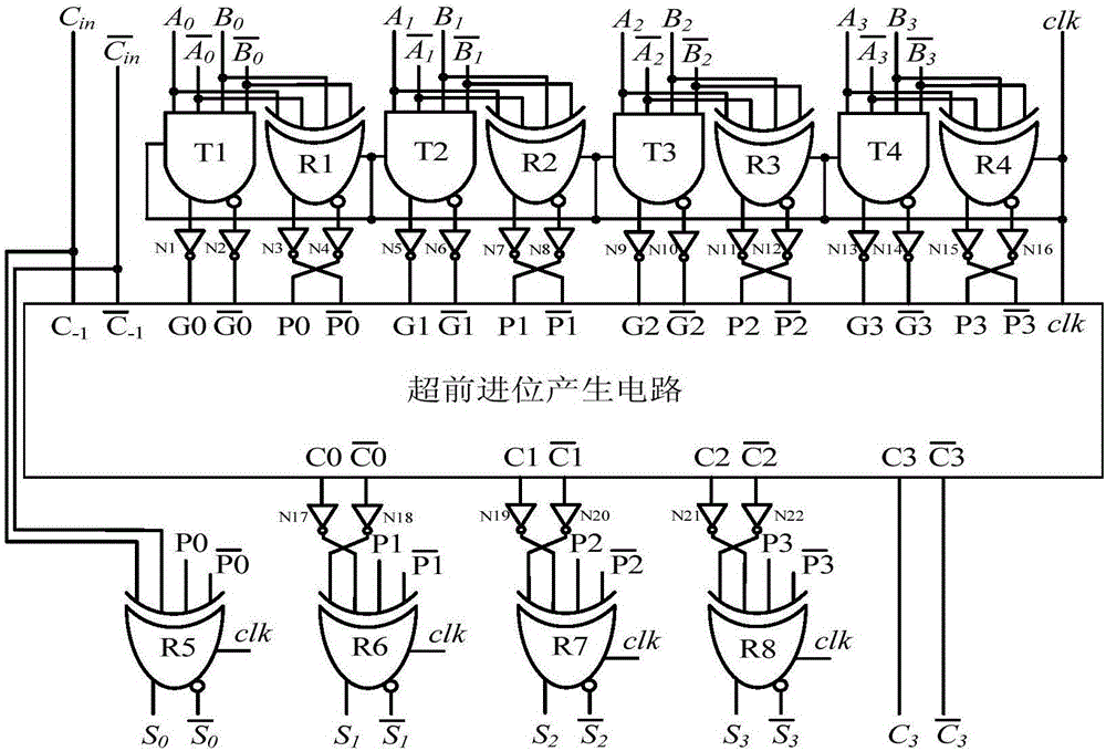
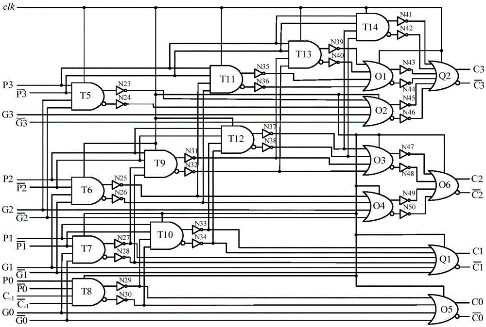
[0029] Embodiment one: if figure 1 , figure 2 with image 3As shown, a defensive differential power consumption analysis adder utilizing sensitive amplified logic includes a first two-input NAND / AND gate T1, a second two-input NAND / AND gate T2, a third two-input NAND / AND gate Gate T3, the fourth two-input NAND / AND gate T4, the first two-input exclusive-or / same-or gate R1, the second two-input exclusive-or / same-or gate R2, the third two-input exclusive-or / same-or gate R3, The fourth two-input XOR / XOR gate R4, the fifth two-input XOR / XOR gate R5, the sixth second-input XOR / XOR gate R6, the seventh second-input XOR / XOR gate R7, the eighth Two-input XOR / NOR gate R8, first inverter N1, second inverter N2, third inverter N3, fourth inverter N4, fifth inverter N5, sixth inverter N6, seventh inverter N7, eighth inverter N8, ninth inverter N9, tenth inverter N10, eleventh inverter N11, twelfth inverter N12, thirteenth inverter Inverter N13, Fourteenth Inverter N14, Fifteenth Inver...

Embodiment 2

[0030]Embodiment two: this embodiment is basically the same as embodiment one, the difference is that in this embodiment, as shown in Figure 4 (a) and Figure 4 (b), the first two input NAND / AND gate T1 includes the first MOS tube M1, second MOS tube M2, third MOS tube M3, fourth MOS tube M4, fifth MOS tube M5, sixth MOS tube M6, seventh MOS tube M7, eighth MOS tube M8, ninth MOS tube M9, the tenth MOS tube M10, the eleventh MOS tube M11 and the twelfth MOS tube M12; the first MOS tube M1, the second MOS tube M2, the third MOS tube M3 and the fourth MOS tube M4 are all P-type MOS tubes tube, the fifth MOS tube M5, the sixth MOS tube M6, the seventh MOS tube M7, the eighth MOS tube M8, the ninth MOS tube M9, the tenth MOS tube M10, the eleventh MOS tube M11 and the twelfth MOS tube M12 are all N-type MOS transistors; the source of the first MOS transistor M1, the source of the second MOS transistor M2, the source of the third MOS transistor M3, the source of the fourth MOS trans...


PUM


Abstract

The invention discloses a differential power analysis defense adder employing sense amplifier based logic. The adder consists of four two-input not and / and gates, eight two-input exclusive or / nor gates, twenty-two inverters and a carry look-ahead generation circuit. The adder has the advantages that a TSMC 65nm CMOS technology is adopted; simulation analysis is performed on the circuit by a Spectre tool; an experimental result indicates that the adder has a correct logic function; compared with the traditional adder circuit, the adder has the advantage that the power independence can be improved by 97%; and differential power analysis can be effectively defended.

Description

technical field [0001] The invention relates to an adder, in particular to a defensive differential power analysis adder utilizing sensitive amplification logic. Background technique [0002] With the development of integrated circuits and computer technology, cryptographic devices are widely used in smart cards, e-commerce and other fields, which greatly guarantee the security of the system. However, when cryptographic devices process different data, physical information such as energy consumption, running time, and electromagnetic radiation has a certain correlation with the processed data. Therefore, attackers usually use these physical information to attack cryptographic devices to obtain key information, and this method is called Side Channel Attack (SCA). Among a series of side-channel attack techniques, Differential Power Analysis (DPA) technology is a common and effective side-channel attack method, which seriously threatens the security of cryptographic devices. I...

Claims


Application Information

Patent Timeline
IPC IPC(8): G06F7/50H03K19/21
CPCG06F7/50H03K19/21
Inventor 汪鹏君钱浩宇张跃军丁代鲁
Owner NINGBO UNIV
Learn More