

dmos device manufacturing method and dmos device
A manufacturing method and device technology, applied in the fields of semiconductor/solid-state device manufacturing, semiconductor devices, electrical components, etc., can solve problems such as semiconductor devices not working properly, and achieve the effects of precise control of doping concentration and equivalent resistance.
- Summary
- Abstract
- Description
- Claims
- Application Information
AI Technical Summary
Problems solved by technology
Method used
Image

Examples
Embodiment 1
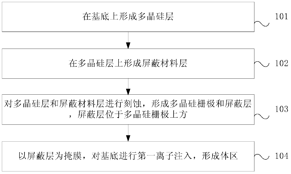
[0022] This embodiment provides a method for fabricating a DMOS device, which is used for fabricating a DMOS device. Such as figure 1 Shown is a schematic flow chart of the method for fabricating a DMOS device according to this embodiment. The fabrication method of the DMOS device of the present embodiment comprises:
[0023] Step 101, forming a polysilicon layer on a substrate.
[0024] The base of this embodiment may include a substrate, an epitaxial layer, and a gate oxide layer formed sequentially from bottom to top. The method of forming the polysilicon layer may be: forming a polysilicon material layer on the gate oxide layer, and then performing an ion implantation doping process to form the polysilicon layer.
[0025] Step 102, forming a shielding material layer on the polysilicon layer.
[0026] The layer of shielding material may be a silicon dioxide layer. There are many ways to form the shielding material layer. For example, a polysilicon layer is formed by de...
Embodiment 2
[0033] In this embodiment, a further supplementary explanation is given to the method for fabricating the DMOS device in the first embodiment. Such as Figures 2A to 2I Shown is a structural schematic diagram of each step of the DMOS device manufacturing method according to this embodiment. In this embodiment, the method for fabricating an N-type DMOS device is taken as an example for illustration.
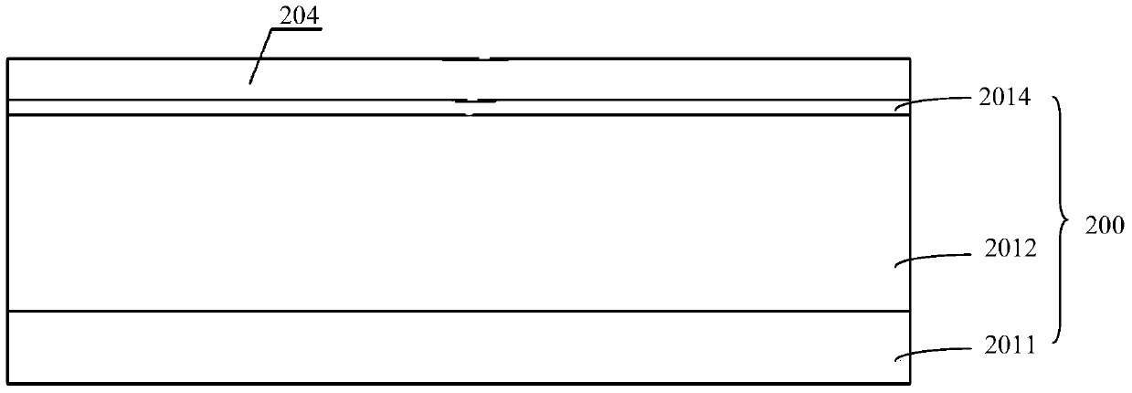
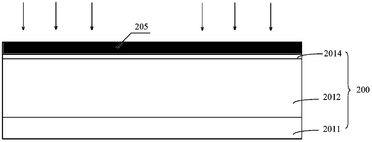
[0034] Such as Figure 2A As shown, a gate oxide layer 2014 is formed on an initial substrate 201 , a substrate 200 is formed from a bottom-up substrate 2011 , an epitaxial layer 2012 and a gate oxide layer 2014 , and then a polysilicon material layer 204 is formed on the substrate 200 .
[0035] The specific method of forming the gate oxide layer 2014 may be thermal oxidation of the epitaxial layer 2012 , and the method of forming the polysilicon material layer 204 may be a deposition method, specifically forming the polysilicon material layer 204 on the gate oxide layer 2014 ....
Embodiment 3
[0056] This embodiment provides a DMOS device. Such as Figure 2E As shown, the DMOS device of this embodiment includes a substrate 200 , a polysilicon gate 207 , a shielding layer 208 and a body region 210 .
[0057] Wherein, the polysilicon gate 207 is formed on the substrate 200 ; the shielding layer 208 is formed above the polysilicon gate 207 ; the body region 210 is formed in the substrate 200 , and the body region 210 is located on both sides of the polysilicon gate 207 . Wherein, the base includes a substrate 2011 , an epitaxial layer 2012 and a gate oxide layer 2014 which are sequentially formed from bottom to top.
[0058] It should be noted that although ions are implanted into the base 210 on both sides of the polysilicon gate 207 , due to ion diffusion in the body region 210 , both ends of the body region 210 will extend into the bottom of the polysilicon gate 207 .
[0059] The material of the shielding layer 208 in this embodiment is silicon dioxide, and the t...
PUM
| Property | Measurement | Unit |
|---|---|---|
| thickness | aaaaa | aaaaa |
Abstract
Description
Claims
Application Information