Polishing pad

A polishing pad and polishing layer technology, applied in the field of polishing pads, can solve the problems of decreased product yield, distribution of polishing liquid, irregular overall structure, etc., and achieve the effects of improving wafer planarization, polishing rate, and simple structure.

Active Publication Date: 2017-04-19
HUBEI DINGLONG CO LTD
View PDF12 Cites 18 Cited by
  • Summary
  • Abstract
  • Description
  • Claims
  • Application Information

AI Technical Summary

Problems solved by technology

Unfortunately, known CMP systems and associated polishing pads are often unable to distribute the polishing fluid in this manner, resulting in uneven removal rates across the wafer surface, overall structural irregularities, unstable wafer uniformity, and reduced product yields

Method used


Image

  • Polishing pad
  • Polishing pad
  • Polishing pad

Examples


Embodiment Construction

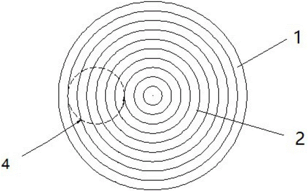
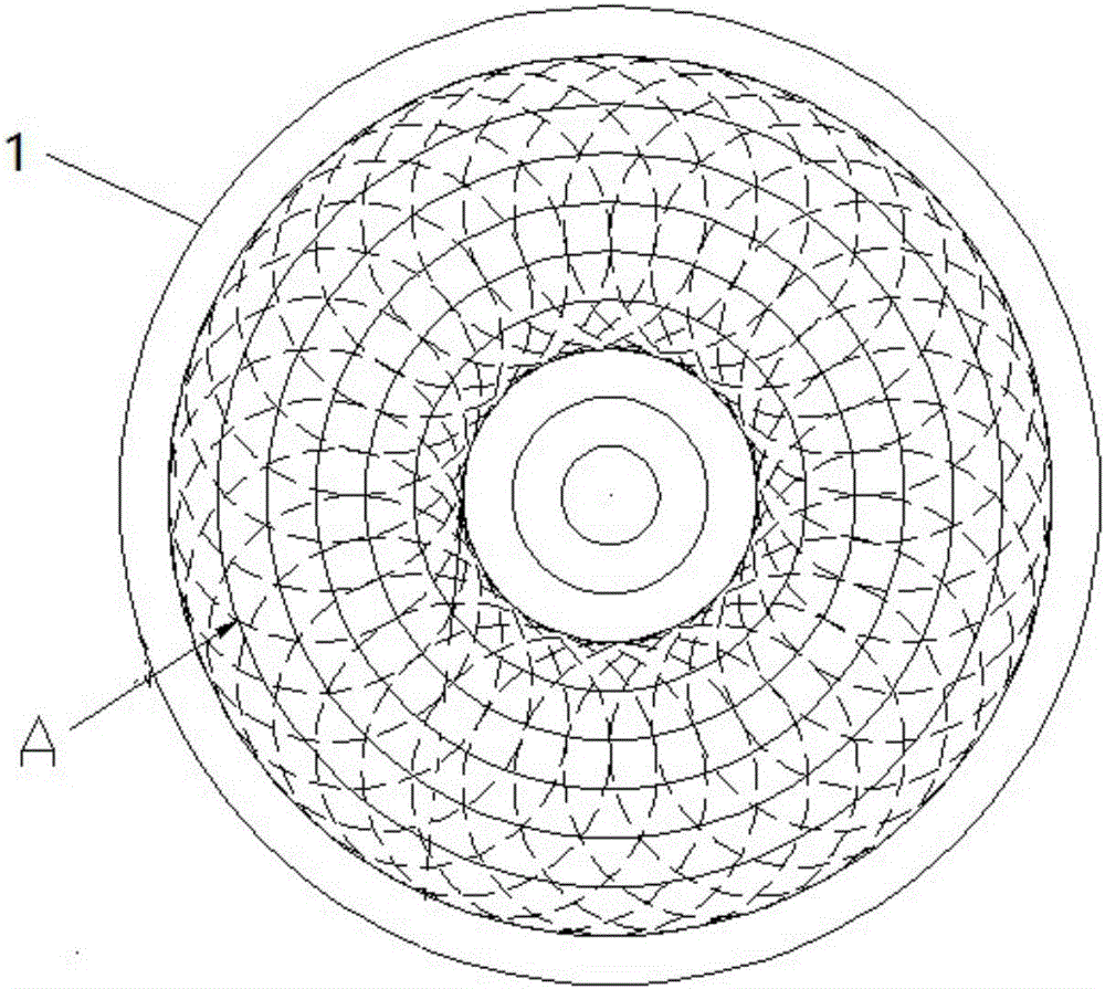
[0036] First, a brief description of the polishing machine, the polishing machine platen can be rotated around its axis of rotation by the platen drive. The wafer can be supported by the wafer carrier and rotated about its axis of rotation. The wafer includes a polished surface, which faces the polishing pad and is planarized during the polishing process. The wafer carrier can be supported by a carrier support assembly, which is suitable for rotating the wafer during the polishing process and provides a downward force F to press the polished surface of the wafer 4 against the polishing pad, so that the polishing surface and the polishing pad There is the required pressure between. The polishing machine is also equipped with a polishing liquid feed port for conveying polishing liquid to the polishing pad. The polishing liquid feeding port should usually be placed at or near the axis of rotation of the polishing machine platen to optimize the polishing effect of the polishing p...


PUM


Abstract

The invention discloses a polishing pad for solving the problems of nonuniform distribution of polishing liquid and need of further improvement of the polishing speed and the leveling degree in a traditional polishing pad. The polishing pad at least comprises a circular polishing layer; a groove for flowing the polishing liquid is formed in the upper surface of the polishing layer; the groove consists of a peripheral groove and a radial groove; the peripheral groove is a peripheral geometric center symmetry pattern with the circle center of the polishing layer as center; the edges m of the pattern are not fewer than 3; and the radial groove is a straight line or/and a curve scattered from the peripheral direction along the circle center, and has an intersecting point with the peripheral groove. The polishing pad is simple in structure, can enable the polishing liquid to uniformly distribute and flow in a polishing area, keeps uniform concentration of reactants and products in the polishing liquid in the polishing area to the greatest extent, accelerates the polishing speed, and improves the wafer planar degree.

Description

Technical field [0001] The present invention relates to the field of chemical mechanical polishing, in particular to a polishing pad used for polishing at least one of a magnetic substrate, an optical substrate and a semiconductor substrate. Background technique [0002] In the manufacturing process of integrated circuits and other electronic devices, multiple layers of conductive, semiconductor and dielectric materials are deposited on the surface of a semiconductor wafer and then removed from the surface of the semiconductor wafer. Many deposition techniques can be used to deposit thin layers of conductive, semiconductor, and dielectric materials. Conventional deposition techniques in modern wafer processing include physical vapor deposition (PVD) (also known as sputtering), chemical vapor deposition (CVD), plasma-assisted chemical vapor deposition (PECVD), and electrochemical plating. Conventional etching techniques include wet and dry isotropic and anisotropic etching. As t...

Claims


Application Information

Patent Timeline
Patent Type & Authority Applications(China)
IPC IPC(8): B24B37/26
CPCB24B37/26
Inventor 朱顺全梅黎黎
Owner HUBEI DINGLONG CO LTD
Why Eureka
Try Eureka