A substrate-integrated waveguide leaky-wave antenna with circularly polarized beam scanning range
A substrate-integrated waveguide and beam scanning technology, applied in leaky waveguide antennas, circuits, etc., to achieve the effects of circularly polarized radiation characteristics optimization, easy design optimization, and simple structure
- Summary
- Abstract
- Description
- Claims
- Application Information
AI Technical Summary
Problems solved by technology
Method used
Image
Examples
specific Embodiment approach 1
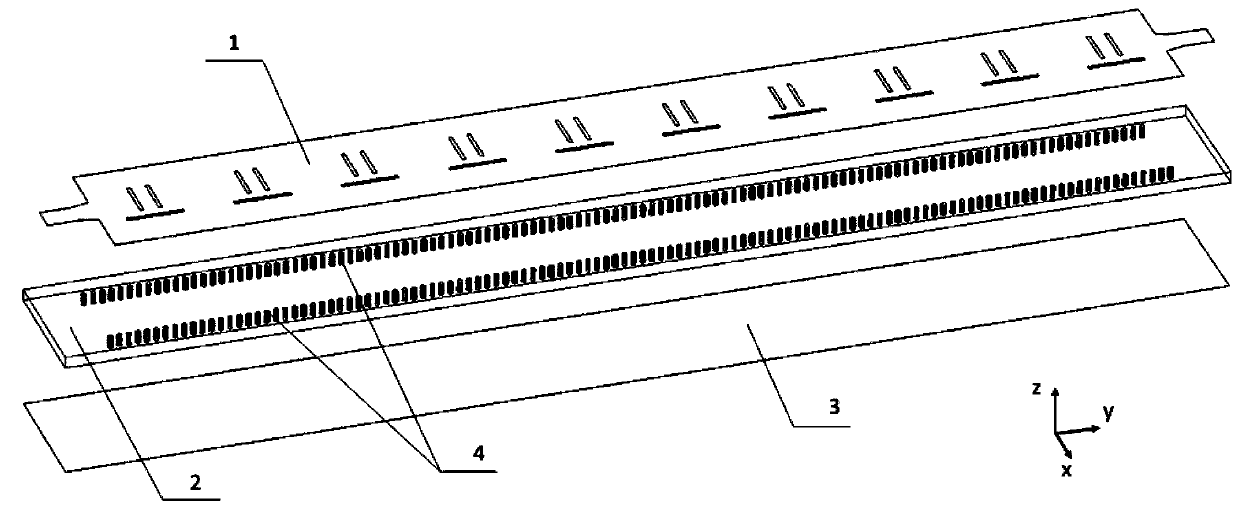
[0033] Specific implementation mode one: the following combination Figure 2 to Figure 5 This embodiment will be described. Depend on figure 2 , the circularly polarized substrate integrated waveguide leaky wave antenna described in this embodiment, its main structure can be divided into three layers - the top metal layer 1, the dielectric substrate layer 2, the bottom metal layer 3 and the double row of metallized via holes 4 ;
[0034] The top metal layer 1 and the bottom metal layer 3 are on the upper and lower sides of the dielectric substrate layer 2, and the three are tightly combined into one body by hot pressing;
[0035] The material of the dielectric substrate layer 2 is a typical microwave plate, the dielectric constant εr is between 2 and 10, and the loss tangent tanδ<0.01;
[0036]Double rows of metallized vias 4 penetrate the dielectric substrate 2, and are metallized by electroplating, so that the top metal layer 1 and the bottom metal layer 3 are electrical...
specific Embodiment approach 2
[0046] Specific implementation mode two: the following combination Figure 6 to Figure 9 This implementation mode is described, and the antenna structure of the first implementation mode is further described in this implementation mode in combination with specific examples.
[0047] As a special case, Figure 6 and Figure 7 The specific design parameters of a circularly polarized substrate-integrated waveguide leaky-wave antenna operating from 10GHz to 14.5GHz are given. Depend on Figure 6 , The dielectric board on the top layer of the antenna is a microwave substrate, the relative permittivity εr = 3.66, the loss tangent tanδ = 0.004, the thickness is ts = 0.762mm, and the thickness of the metal layer tm = 0.035mm. The antenna is composed of N=10 periodic slot units, unit spacing p=14mm, longitudinal slot 1-1 length L=7mm, transverse slot pair 1-2 length T=5.4mm, longitudinal slot 1-1 and transverse slot pair 1 The width of -2 is ws=0.4mm, the slot distance dy=2.4mm in ...
PUM
 Abstract
Description
Claims
Application Information


