Thin film transistor array substrate and preparation method thereof, and display device

A technology for thin film transistors and array substrates, applied in the field of display manufacturing, can solve problems such as electrical failure, thin film transistor threshold voltage drift, and reduce product yield, and achieve the effects of preventing threshold voltage drift and improving yield

Inactive Publication Date: 2017-04-26
TCL CHINA STAR OPTOELECTRONICS TECH CO LTD
View PDF2 Cites 16 Cited by
  • Summary
  • Abstract
  • Description
  • Claims
  • Application Information

AI Technical Summary

Problems solved by technology

[0004] However, at present, when IGZO is used in the preparation process of thin film transistors, it is greatly affected by light, heat and electricity. Among them, after the preparation of the active layer is completed, the photomask technology used in the subsequent manufacturing process may cause the active layer to be affected by the light. It is easy to cause threshold voltage drift of thin film transistors, electrical failure, and lower product yield

Method used


Image

  • Thin film transistor array substrate and preparation method thereof, and display device
  • Thin film transistor array substrate and preparation method thereof, and display device
  • Thin film transistor array substrate and preparation method thereof, and display device

Examples


Embodiment 1

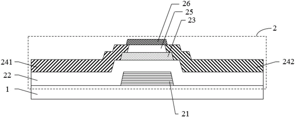
[0025] Such as figure 1 As shown, this embodiment provides a thin film transistor array substrate, which includes a plurality of thin film transistors 2 arranged in an array on a glass substrate 1, and only one thin film transistor 2 is shown here as an example to more clearly describe the The structure of the thin film transistor.

[0026] The thin film transistor 2 includes: a gate electrode 21, a gate insulating layer 22 covering the gate electrode 21, an active layer 23 formed on the gate insulating layer 22, a source electrode 241 and a drain electrode 242 , the source electrode 241 and the drain electrode 242 are spaced from each other and part of the structure is overlapped on the active layer 23, and the active layer 23 corresponds to the distance between the source electrode 241 and the drain electrode 242. region forms the channel region.

[0027] Specifically, the material of the active layer 23 is a metal oxide semiconductor material. Compared with amorphous sil...

Embodiment 2

[0048] Embodiment 2 provides a display device, wherein the thin film transistor array substrate provided in Embodiment 1 is used. By adopting the thin film transistor array substrate as provided in Embodiment 1, the display device can have the advantages brought by the above thin film transistor array substrate.

[0049] Specifically, a thin film transistor liquid crystal display device is used as an example showing the application of the above thin film transistor array substrate to a display device, see Figure 4 The liquid crystal display device includes a liquid crystal panel 100 and a backlight module 200, the liquid crystal panel 100 is arranged opposite to the backlight module 200, and the backlight module 200 provides a display light source to the liquid crystal panel 100, so that the The liquid crystal panel 100 displays images. Wherein, the liquid crystal panel 100 includes an array substrate 101 and a filter substrate 102 disposed opposite to each other, and furthe...


PUM


Abstract

The invention discloses a thin film transistor array substrate. In a thin film transistor of the array substrate, the material of an active layer is a metal oxide semiconductor material, an etching barrier layer is also arranged on the active layer, the etching barrier layer covers a channel region, and a light shielding layer is also arranged on the etching barrier layer. The method for preparing the abovementioned thin film transistor array substrate includes preparing and obtaining the etching barrier layer and the light shielding layer in a same photomask process. In addition, the invention also discloses a display device including the abovementioned thin film transistor array substrate. In the thin film transistor array substrate provided by the invention, through additional arrangement of the light shielding layer, influence of illumination on the active layer of the thin film transistor in a manufacture process is avoided, and the problems of threshold voltage drifting and electrical property failure of the thin film transistor due to illumination influence are prevented, thereby improving product quality.

Description

technical field [0001] The present invention relates to the technical field of display manufacturing, in particular to a thin film transistor array substrate and a preparation method thereof, and also to a display device including the array substrate. Background technique [0002] The flat panel display device has many advantages such as thin body, power saving, and no radiation, and has been widely used. The core component of the flat panel display device is a thin film transistor TFT (Thin Film Transistor). Using semiconductor oxide as the active layer to make TFTs for flat panel display devices can not only obtain high mobility, but also has a relatively simple manufacturing process and can be performed at a lower temperature, which has broad application prospects. [0003] IGZO (Indium Gallium Zinc Oxide) is indium gallium zinc oxide. Amorphous IGZO material is a channel layer material used in a new generation of thin film transistor technology, and is a kind of metal o...

Claims


Application Information

Patent Timeline
Patent Type & Authority Applications(China)
IPC IPC(8): H01L27/12
CPCH01L27/1214H01L27/1288
Inventor 甘启明
Owner TCL CHINA STAR OPTOELECTRONICS TECH CO LTD
Why Eureka
Try Eureka