OLED substrate and manufacturing method thereof

一种制作方法、基板的技术,应用在最终产品制造、可持续制造/加工、半导体/固态器件制造等方向,能够解决像素定义层的表面疏水性不够理想、工艺复杂、混色等问题,达到优异疏水特性、色纯度高的效果

Inactive Publication Date: 2017-04-26
TCL CHINA STAR OPTOELECTRONICS TECH CO LTD
View PDF5 Cites 12 Cited by
  • Summary
  • Abstract
  • Description
  • Claims
  • Application Information

AI Technical Summary

Problems solved by technology

In order to achieve the absolute hydrophobic effect on the surface of the pixel definition layer, the commonly used technical means is to add hydrophobic substances to ordinary organic photoresist materials to obtain hydrophobic organic photoresist materials, and then use the hydrophobic organic photoresist materials to make pixel definition layers. layer, the surface of the final pixel definition layer has hydrophobic properties, but this method is complicated, and the surface hydrophobicity of the pixel definition layer is often not ideal, and it cannot effectively solve the problem of staying on the top of the pixel definition layer when printing OLED materials. or cause color mixing problems

Method used


Image

  • OLED substrate and manufacturing method thereof
  • OLED substrate and manufacturing method thereof
  • OLED substrate and manufacturing method thereof

Examples


Embodiment Construction

[0032] In order to further illustrate the technical means adopted by the present invention and its effects, the following describes in detail in conjunction with preferred embodiments of the present invention and accompanying drawings.

[0033] see figure 1 , the invention provides a method for manufacturing an OLED substrate, comprising the following steps:

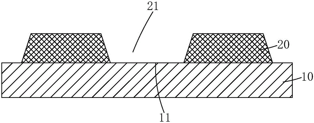
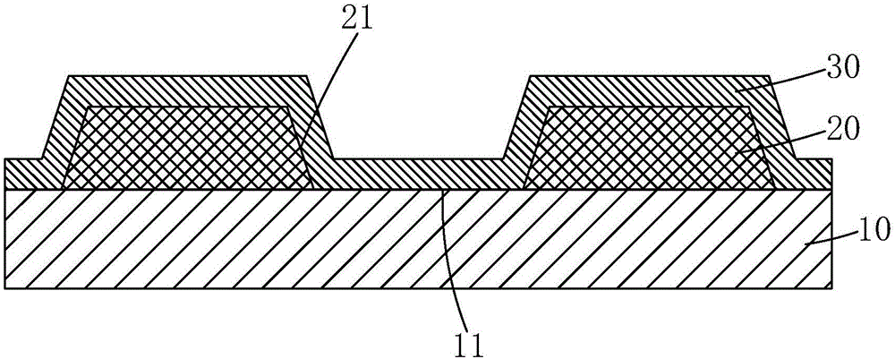
[0034] Step 1, such as figure 2 As shown, a base substrate 10 is provided, and a pixel definition layer 20 is formed on the base substrate 10, and several through holes 21 are arranged on the pixel definition layer 20, and the several through holes 21 are formed on the base substrate. Several pixel areas 11 are respectively defined on 10 .

[0035] Specifically, the base substrate 10 is a TFT substrate.

[0036] Specifically, the material of the pixel definition layer 20 is common organic photoresist, and the common organic photoresist material has a certain degree of hydrophobicity, but the hydrophobicity is poor en...


PUM


Abstract

The invention provides an OLED substrate and a manufacturing method thereof. According to the manufacturing method of the OLED substrate, a silicon membrane is arranged on the top surface of a pixel defining layer, the top surface of the pixel defining layer is enabled to have an excellent hydrophobic feature, and when ink-jet printing of an OLED material is carried out in a pixel area of a substrate, the OLED material wrongly sprayed to the silicon membrane on the top surface of the pixel defining layer does not stay on the silicon membrane but rapidly slides off to the pixel area of the substrate, such that the problem of color mixing caused when the OLED material stays on the top surface of the pixel defining layer and even slides off to an adjacent pixel area is avoided effectively. According to the OLED substrate, the color purity of an OLED luminescent layer is high, and the problem of color mixing is not generated.

Description

technical field [0001] The invention relates to the field of display technology, in particular to an OLED substrate and a manufacturing method thereof. Background technique [0002] Organic Light Emitting Display (OLED) has self-illumination, low driving voltage, high luminous efficiency, short response time, high definition and contrast, nearly 180° viewing angle, wide operating temperature range, and can realize flexible display and With many advantages such as large-area full-color display, it is recognized by the industry as a display device with the most potential for development. [0003] According to the driving method, OLED can be divided into two categories: passive matrix OLED (Passive Matrix OLED, PMOLED) and active matrix OLED (Active Matrix OLED, AMOLED), namely direct addressing and thin film transistor matrix addressing. Among them, AMOLED has pixels arranged in an array, belongs to the active display type, has high luminous efficiency, and is usually used as...

Claims


Application Information

Patent Timeline
Patent Type & Authority Applications(China)
IPC IPC(8): H01L27/32H01L51/52H01L51/56H01L21/77
CPCH10K59/122H10K71/135H10K50/86H10K50/844H10K59/1201H10K71/00Y02E10/549Y02P70/50H10K59/173H10K77/10H01L27/1218
Inventor 张晓星
Owner TCL CHINA STAR OPTOELECTRONICS TECH CO LTD
Why Eureka
Try Eureka