Semiconductor element and its manufacturing method
A semiconductor and component technology, applied in the field of high-voltage semiconductor components and their manufacturing, can solve the problems of snapback breakdown, component reliability and service life reduction, etc. Effect
Active Publication Date: 2019-11-12
POWERCHIP SEMICON MFG CORP
View PDF4 Cites 0 Cited by
- Summary
- Abstract
- Description
- Claims
- Application Information
AI Technical Summary
Problems solved by technology
In more severe cases, the drain saturation current (I dsat ) will even appear snapback (snapback), which will lead to the occurrence of snapback breakdown (snapback breakdown), which will reduce the reliability and service life of components
Method used
View moreImage
Smart ImageViewing Examples

Examples
experiment example
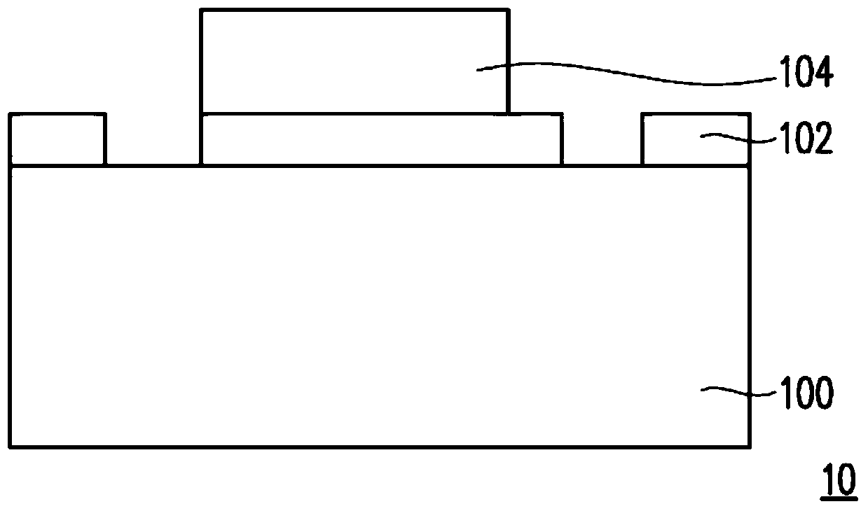
[0061] An experimental example of a semiconductor device fabricated according to an embodiment of the present invention is simulated. In this experimental example, the substrate of the semiconductor element includes a source region and a drain region, the distance between the source region and the drain region is 2.5 μm to 4 μm (ie the second width L2 ), and the gate of the semiconductor element has Two gate doped regions and one gate undoped region, the gate undoped region is located between the two gate doped regions to separate them, and the gate undoped region has a width of 0.2 μm (ie first width L1).
Login to View More PUM
 Abstract
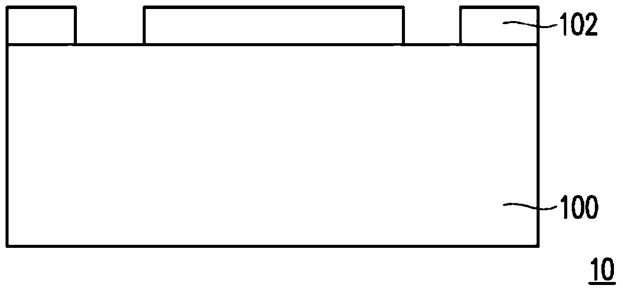
The invention discloses a semiconductor element and a manufacturing method thereof. The manufacturing method includes the following steps and provides a substrate. A gate dielectric layer is formed to cover a portion of the substrate. The gate electrode is formed on the gate dielectric layer. A first doping process is performed on a portion of the gate to form a plurality of gate doped regions and at least one gate undoped region on the gate, and the at least one gate undoped region is located between the gate doped regions, and The sum of the widths of the at least one gate undoped region is a first width. A dielectric layer is formed to cover the top surface and sidewalls of the gate. A second doping process is performed on the substrate to form a source region and a drain region, where the shortest distance between the source region and the drain region is the second width.
Description
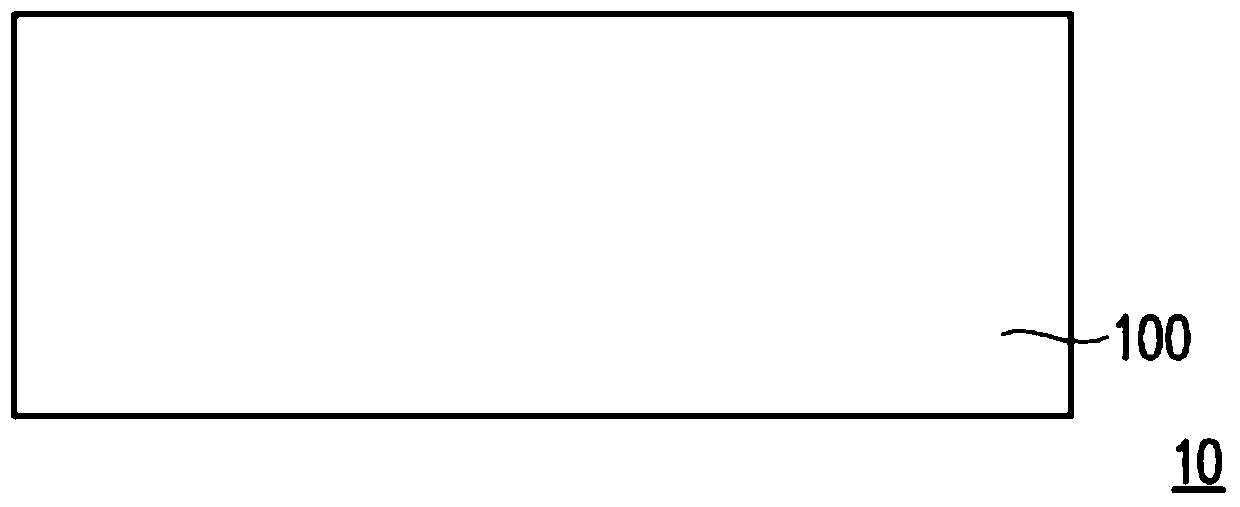
technical field [0001] The present invention relates to a semiconductor element and a manufacturing method thereof, and in particular, to a high-voltage semiconductor element and a manufacturing method thereof. Background technique [0002] With the integration of semiconductor elements, in order to achieve the goals of high density and high performance, when manufacturing semiconductor elements, there is a tendency to manufacture smaller and more highly integrated structures. However, as the device size shrinks, the problem of hot carrier effect still exists. In more severe cases, the drain saturation current (I dsat ), a snapback may even occur, resulting in a snapback breakdown phenomenon, which will reduce the reliability and service life of the components. This type of problem is more severe in high voltage devices. Therefore, how to reduce the snapback breakdown caused by the hot carrier effect is a subject that needs to be studied at present. SUMMARY OF THE INVEN...
Claims
Login to View More Application Information
Patent Timeline
 Patent Type & Authority Patents(China)
IPC IPC(8): H01L29/772H01L21/335
CPCH01L29/66409H01L29/772
Inventor 彭康钧车行远李芃葳
Owner POWERCHIP SEMICON MFG CORP