A Mixer Circuit of CMOS Complementary Structure
A mixer and circuit technology, applied in electrical components, modulation conversion balance devices, demodulation, etc., to achieve the effects of reducing power consumption, reducing requirements, and relieving design pressure
- Summary
- Abstract
- Description
- Claims
- Application Information
AI Technical Summary
Problems solved by technology
Method used
Image

Examples
Embodiment Construction
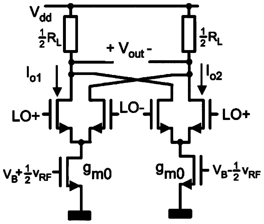
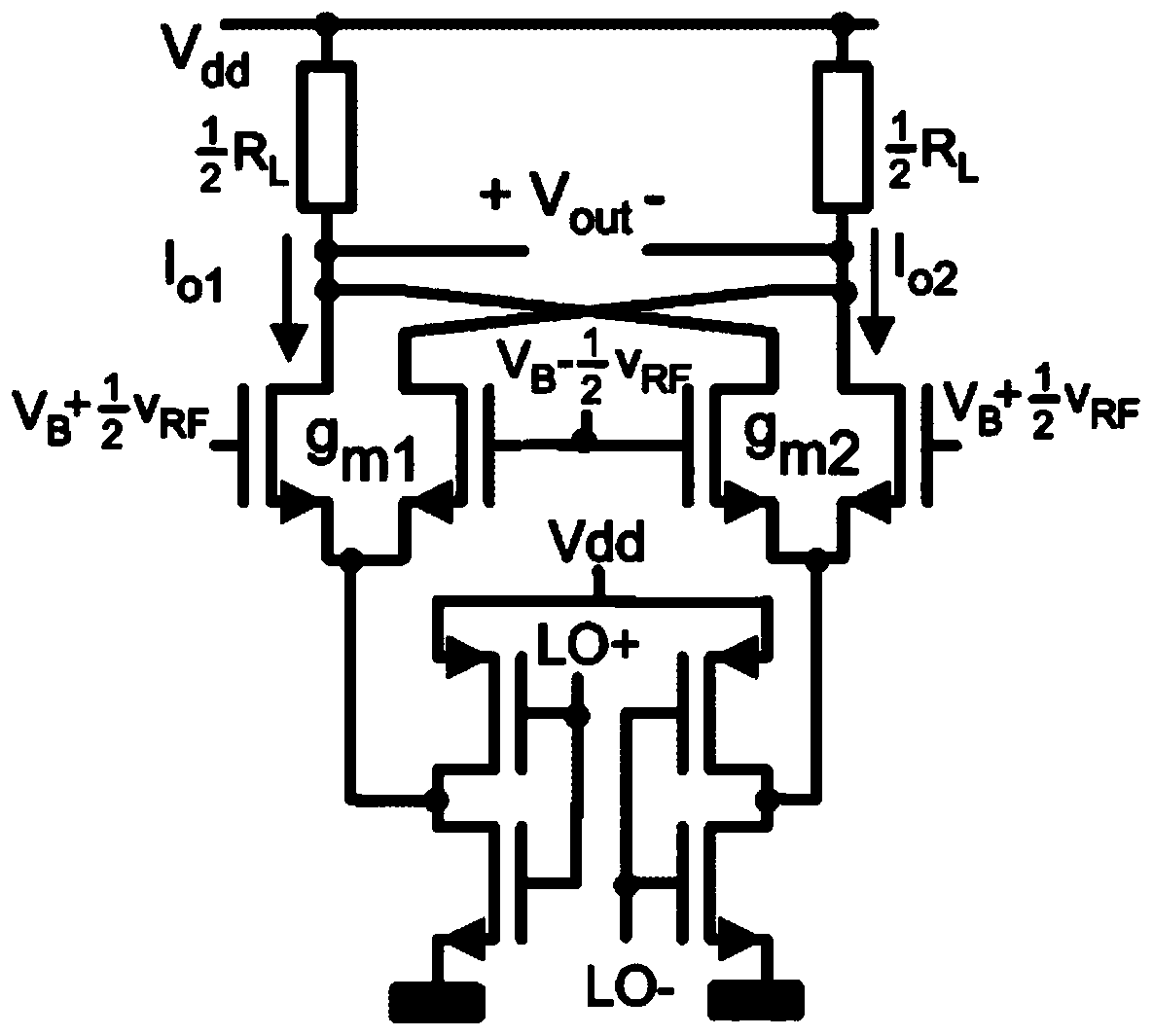
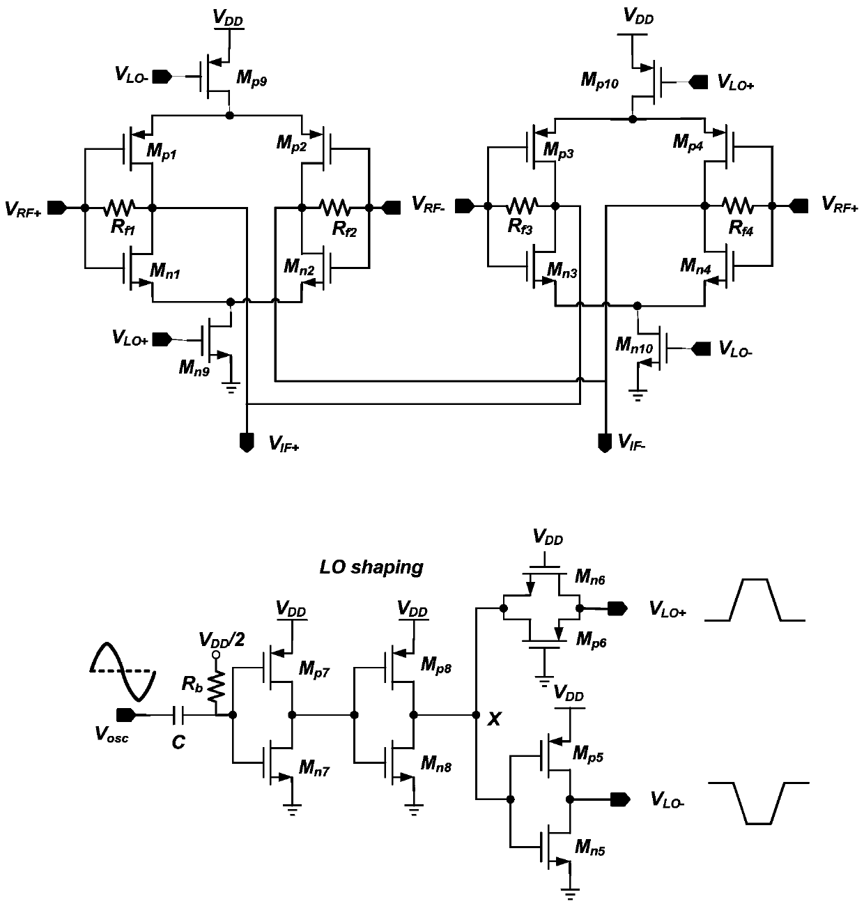
[0030] In order to facilitate those skilled in the art to understand the technical content of the present invention, the content of the present invention will be further explained below in conjunction with the accompanying drawings.
[0031] Such as image 3 Shown is a mixer circuit diagram of a CMOS complementary structure of the present invention, including: a first transconductance input stage, a second transconductance input stage, a third transconductance input stage, a fourth transconductance input stage, a local oscillator pulse Shaping stage, first resistor, second resistor, third resistor, fourth resistor, ninth NMOS transistor, ninth PMOS transistor, tenth NMOS transistor, tenth PMOS transistor.
[0032] The first transconductance input stage, the second transconductance input stage, the third transconductance input stage, and the fourth transconductance input stage receive the RF voltage signal, and the RF voltage signal V RF+ or V RF- converted to a current signa...
PUM
 Abstract
Description
Claims
Application Information
 - R&D
- Intellectual Property
- Life Sciences
- Materials
- Tech Scout
- Unparalleled Data Quality
- Higher Quality Content
- 60% Fewer Hallucinations
Browse by: Latest US Patents, China's latest patents, Technical Efficacy Thesaurus, Application Domain, Technology Topic, Popular Technical Reports.
© 2025 PatSnap. All rights reserved.Legal|Privacy policy|Modern Slavery Act Transparency Statement|Sitemap|About US| Contact US: help@patsnap.com