
Formation method of contact hole

A contact hole and cushion technology, which is applied in the direction of semiconductor/solid-state device components, electrical components, circuits, etc., can solve the problems of increased contact hole resistance, and achieve the effect of avoiding damage.

Active Publication Date: 2020-05-08
SEMICON MFG INT (SHANGHAI) CORP +1
View PDF3 Cites 0 Cited by
  • Summary
  • Abstract
  • Description
  • Claims
  • Application Information

AI Technical Summary

Problems solved by technology

[0003] However, when the barrier layer is deposited, a part of the barrier layer will also be deposited at the bottom of the through hole, and the barrier layer at the bottom of the through hole will lead to an increase in the resistance of the contact hole, so a method for reducing the contact resistance of the contact hole is needed

Method used


Image

  • Formation method of contact hole
  • Formation method of contact hole
  • Formation method of contact hole

Examples


Embodiment Construction

[0025] Embodiments of the present invention provide a method for forming a contact hole, which will be described in detail below with reference to the accompanying drawings:

[0026] It should be noted that in this embodiment, the formation of a single damascene structure is taken as an example for illustration, and the method of the present invention can also be applied to other via structures, such as plug or straight via structures, which will not be listed here.

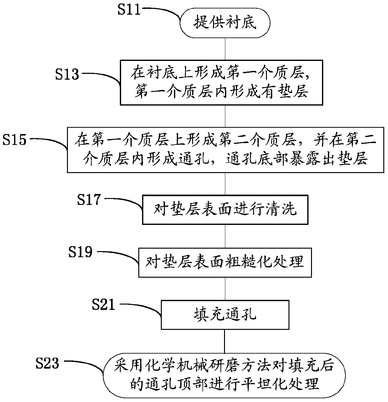
[0027] refer to figure 1 In step S11 and Figure 4 , providing a semiconductor substrate 10 .

[0028] The semiconductor substrate 10 can be single crystal silicon or polycrystalline silicon; the semiconductor substrate 10 can also be selected from silicon, germanium, gallium arsenide or silicon germanium compound; the semiconductor substrate 10 can also be other semiconductor materials; The semiconductor substrate 10 can also be selected from having an epitaxial layer or a silicon-on-epitaxial structure; and a...


PUM


Abstract

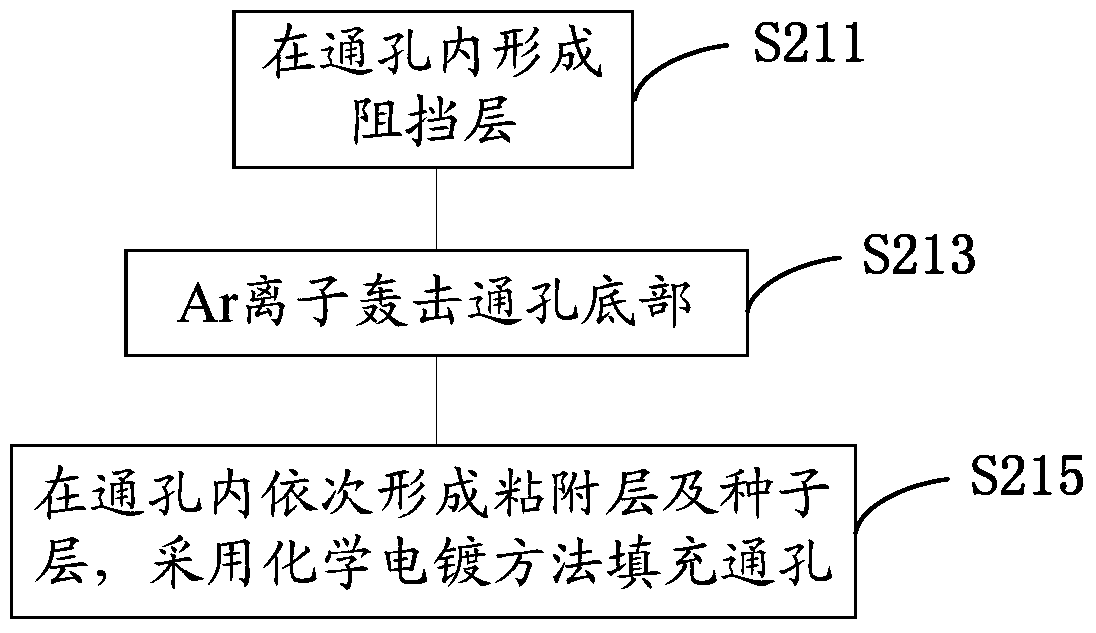
A method for forming a contact hole, comprising: providing a base, and a pad layer is formed in the base; forming a dielectric layer, and the dielectric layer covers the base and the pad layer; The pad layer is exposed at the bottom of the through hole; the surface of the exposed pad layer is treated to make it rough; and a conductive material is filled in the through hole to form a contact hole. In the present invention, the surface of the cushion layer exposed at the bottom of the through hole is roughened, so that the bonding force between the subsequently formed barrier layer and the surface of the cushion layer is weakened, under the premise of protecting the dielectric layer from damage , it is easier to reduce the thickness of the barrier layer at the bottom of the through hole through technological means, thereby effectively reducing the contact resistance of the contact hole.

Description

technical field [0001] The invention relates to the field of semiconductor manufacturing, in particular to a method for forming a contact hole. Background technique [0002] In integrated circuit technology, contact holes are usually used to realize the interconnection between the upper and lower layers. The specific process includes: firstly depositing the dielectric layer; then using photolithography and etching to form through holes; then using physical vapor deposition (Physical Vapor Deposition, PVD) technology to form barrier layers and seed layers in turn; and then using electrochemical plating (Electro chemicalplating) , ECP) ​​method to fill the through hole; use chemical mechanical polishing (Chemical Mechanical Polishing, CMP) method to planarize the top of the filled through hole. [0003] However, when the barrier layer is deposited, a part of the barrier layer is also deposited at the bottom of the through hole, and the barrier layer at the bottom of the throu...

Claims


Application Information

Patent Timeline
Patent Type & Authority Patents(China)
IPC IPC(8): H01L21/768
CPCH01L21/76801H01L21/76831H01L21/76814H01L21/76844H01L21/02063H01L21/321H01L21/32131H01L21/32134H01L21/32135H01L21/76843H01L21/76804H01L21/76826H01L21/76883H01L23/5226H01L23/5283H01L23/53295
Inventor 刘继全
Owner SEMICON MFG INT (SHANGHAI) CORP
Learn More