Display panel, display apparatus and preparation method for display panel

A display panel and display area technology, applied in semiconductor/solid-state device manufacturing, semiconductor/solid-state device components, semiconductor devices, etc., can solve problems such as prone to bending cracks, affecting packaging effects, and small elastic modulus of inorganic layers , to improve the ability to resist bending stress and cutting stress, improve the risk of cracks, and improve the effect of packaging

Active Publication Date: 2017-05-10
WUHAN TIANMA MICRO ELECTRONICS CO LTD
View PDF3 Cites 86 Cited by
  • Summary
  • Abstract
  • Description
  • Claims
  • Application Information

AI Technical Summary

Problems solved by technology

Because the inorganic layer has a dense film structure, it mainly plays the role of blocking water and oxygen, but because the elastic modulus of the inorganic layer is small, bending cracks or cutting cracks are prone to occur, so an organic layer is arranged between the inorganic layers to relieve the inorganic layer. interlayer stress, figure 1 It is a structural schematic diagram of a display panel in the prior art, including a substrate 10', an organic light-emitting device 20' and a thin film encapsulation layer 30', wherein the thin film encapsulation layer 30' includes a first inorganic encapsulation layer 31', an organic encapsulation layer 32' In direct contact with the second inorganic encapsulation layer 33', the two inorganic encapsulation layers 31' and 33' are in direct contact with the edge area 1 of the display panel. As the number of times of bending of the flexible display panel increases, cracks are more likely to occur in this area, affecting Encapsulation effect

Method used


Image

  • Display panel, display apparatus and preparation method for display panel
  • Display panel, display apparatus and preparation method for display panel
  • Display panel, display apparatus and preparation method for display panel

Examples


Embodiment Construction

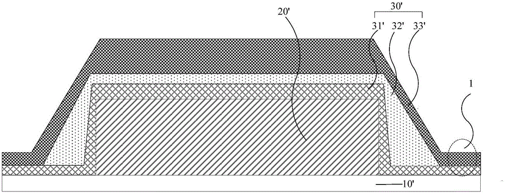
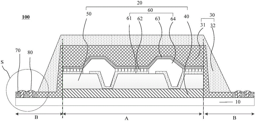
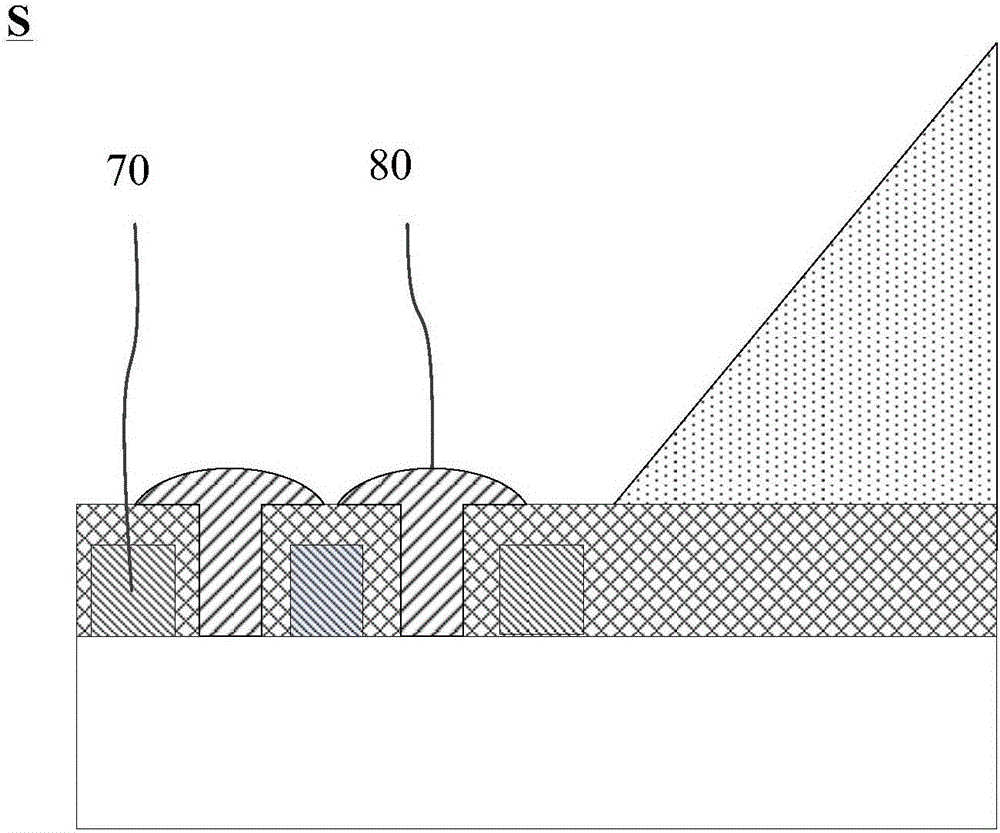
[0028] In order to make the above objects, features and advantages of the present invention more comprehensible, the present invention will be further described below in conjunction with the accompanying drawings and embodiments. Example embodiments may, however, be embodied in many forms and should not be construed as limited to the embodiments set forth herein; rather, these embodiments are provided so that this disclosure will be thorough and complete, and will fully convey the concept of example embodiments to those skilled in the art. The same reference numerals denote the same or similar structures in the drawings, and thus their repeated descriptions will be omitted. The words expressing position and direction described in the present invention are all described by taking the accompanying drawings as an example, but changes can also be made according to needs, and all changes are included in the protection scope of the present invention. The accompanying drawings of th...


PUM


Abstract

The invention discloses a display panel, a display apparatus and a preparation method for the display panel. The display panel comprises a substrate, an organic light emitting device, a thin film packaging layer, and a metal layer, wherein the substrate comprises a display region and a non-display region; the organic light emitting device is arranged in the display region of the substrate; the thin film packaging layer covers the organic light emitting device; the metal layer is positioned in the non-display region of the substrate; grooves are formed in the metal layer; and the grooves are filled with an organic layer. By virtue of setting the metal layer in the non-display region of the substrate, forming the grooves in the metal layer and filling the grooves with the organic layer, bending stress resistance and cutting stress resistance of an edge region are improved, so that risk of cracks on the edge is relieved, and crack expansion can be effectively prevented.

Description

technical field [0001] The present invention relates to the field of display technology, in particular to a display panel, a display device including the display panel, and a manufacturing method of the display panel. Background technique [0002] With the continuous development of display technology, the display panel manufacturing technology is becoming more and more mature. Existing display panels mainly include Organic Light Emitting Diode (OLED), Liquid Crystal Display (LCD), A plasma display panel (Plasma Display Panel, PDP) and the like. The flexible display panel is a deformable and bendable display panel made of materials such as polyimide or polyester film. Compared with the traditional display panel, the flexible display panel has the advantages of small size, low power consumption, With the advantages of being bendable and flexible, it is a display panel with broad application prospects. [0003] Existing flexible display panels usually use thin film packaging ...

Claims


Application Information

Patent Timeline
Patent Type & Authority Applications(China)
IPC IPC(8): H01L27/32H01L23/00H01L51/56
CPCH01L23/562H10K59/12H10K71/00
Inventor 金健苏聪艺
Owner WUHAN TIANMA MICRO ELECTRONICS CO LTD
Why Eureka
Try Eureka