Check patentability & draft patents in minutes with Patsnap Eureka AI!

Method for manufacturing semiconductor power device

A technology of power devices and manufacturing methods, which is applied in the direction of semiconductor devices, electrical components, circuits, etc., can solve the problems of increasing the manufacturing cost of semiconductor power devices and increasing the difficulty of process control, etc., to achieve easy control, simple and reliable process, and reduce manufacturing difficulty Effect

Inactive Publication Date: 2017-05-10
SUZHOU ORIENTAL SEMICONDUCTOR CO LTD
View PDF6 Cites 0 Cited by
  • Summary
  • Abstract
  • Description
  • Claims
  • Application Information

AI Technical Summary

Problems solved by technology

[0003] In the existing manufacturing method of trench type semiconductor power devices, after forming the control gate, the position of the source region is defined by a one-step photolithography process, and then the source region is formed by ion implantation, which requires an additional source region light source. The engraved mask plate and one-step photolithography process increase the manufacturing cost of semiconductor power devices; and as the size of semiconductor power devices continues to shrink, the requirements for photolithography registration accuracy in the source area are gradually increasing, and the difficulty of process control is increasing

Method used


Image

  • Method for manufacturing semiconductor power device
  • Method for manufacturing semiconductor power device
  • Method for manufacturing semiconductor power device

Examples


Embodiment Construction

[0034] The specific implementation manners of the present invention will be further described in detail below in conjunction with the drawings and examples.

[0035] For convenience of illustration, the thicknesses of layers and regions are exaggerated in the drawings, and the shown sizes do not represent actual sizes. Although the shown drawings do not completely and accurately reflect the actual size of the device, they still completely reflect the mutual positions between the regions and the constituent structures, especially the upper-lower and adjacent relationships among the constituent structures. Embodiments of the present invention described below should not be considered limited to the specific shapes of regions shown in the drawings but include resulting shapes such as manufacturing-induced deviations and the like.

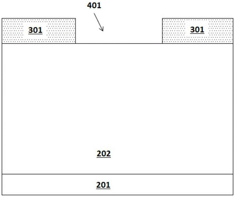
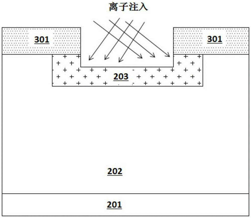
[0036] combine Figure 1 to Figure 7 The technical process of the first scheme of the manufacturing method of a semiconductor power device proposed by ...


PUM


Abstract

The invention belongs to the technical filed of manufacture of semiconductor power devices, and particularly relates to a method for manufacturing a semiconductor power device. According to the method, before a control gate is formed, inclined ion implantation and high-temperature annealing processes are performed, then a method of etching to form a control gate groove is adopted to form a source region, and a photoetching process of a source region in a traditional manufacturing process of a semiconductor power device can be abolished. The technological process of the method for manufacturing the semiconductor power device is simple and reliable and is easy to control, the manufacturing cost of the semiconductor power device can be greatly reduced, and the manufacturing difficulty of the semiconductor power device can also be reduced.

Description

technical field [0001] The invention belongs to the technical field of manufacturing semiconductor power devices, in particular to a method for manufacturing semiconductor power devices. Background technique [0002] With the continuous and in-depth development of microelectronics technology, power MOS transistors achieve high current due to their high input impedance, low loss, fast switching speed, no secondary breakdown, wide safe working area, good dynamic performance, and easy coupling with the front electrode. , high conversion efficiency and other advantages, gradually replacing bipolar devices has become the mainstream of the development of semiconductor power devices today. Commonly used power MOS transistors mainly include planar diffusion power devices and trench power devices. Because the trench type power device adopts a vertical channel structure, its area is much smaller than that of the planar diffusion type power device, so its current density is greatly im...

Claims


Application Information

Patent Timeline
IPC IPC(8): H01L29/66
CPCH01L29/66666
Inventor 毛振东刘伟刘磊
Owner SUZHOU ORIENTAL SEMICONDUCTOR CO LTD
Features
  • R&D
  • Intellectual Property
  • Life Sciences
  • Materials
  • Tech Scout
  • Unparalleled Data Quality
  • Higher Quality Content
  • 60% Fewer Hallucinations
Learn More