Phase change material layer, phase change memory unit and preparation method thereof

A phase-change memory and phase-change material technology, which is applied in the field of semiconductor material preparation, can solve the problems of slow phase change and short life of storage devices, and achieve good adhesion, prolong life, and improve thermal stability.

Active Publication Date: 2019-04-16
SHANGHAI INST OF MICROSYSTEM & INFORMATION TECH CHINESE ACAD OF SCI
View PDF6 Cites 0 Cited by
  • Summary
  • Abstract
  • Description
  • Claims
  • Application Information

AI Technical Summary

Problems solved by technology

[0005] In view of the shortcomings of the prior art described above, the purpose of the present invention is to provide a phase change memory unit and its preparation method, which are used to solve the problems of slow phase transition speed and short lifespan of storage devices in the prior art

Method used


Image

  • Phase change material layer, phase change memory unit and preparation method thereof
  • Phase change material layer, phase change memory unit and preparation method thereof
  • Phase change material layer, phase change memory unit and preparation method thereof

Examples


Embodiment 1

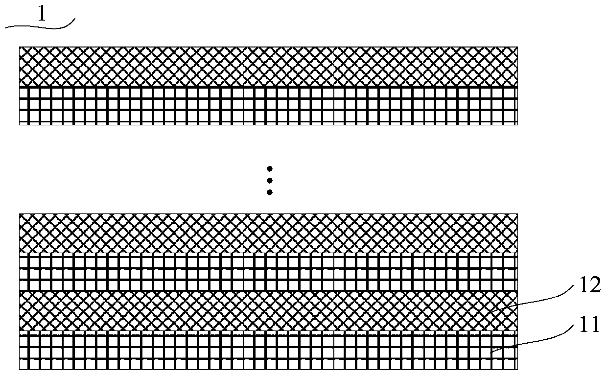
[0061] see figure 1 , the present invention provides a phase change material layer 1, the phase change material layer 1 includes Ti x Te 1-x layer 11 and located on the Ti x Te 1-x The Sb layer 12 on the surface of the layer 11, wherein 0.33≤x≤0.56.

[0062] As an example, the Ti x Te 1-x The thickness of the layer 11 is 1 nm to 10 nm, and the thickness of the Sb layer 12 is 1 nm to 10 nm; preferably, in this embodiment, the Ti x Te 1-x Layer 11 has a thickness of 3 nm and said Sb layer 12 has a thickness of 8 nm.

[0063] As an example, the phase change material layer 1 includes a plurality of Ti x Te 1-x layer 11 and a plurality of the Sb layers 12, the Ti x Te 1-x Layer 11 and the Sb layer 12 are alternately stacked to form a phase-change superlattice film structure, and the bottom layer of the phase-change material layer 1 is the Ti x Te 1-x Layer 11.

[0064] As an example, the Ti x Te 1-x The layer 11 and the Sb layer 12 are alternately stacked for 3-25 p...

Embodiment 2

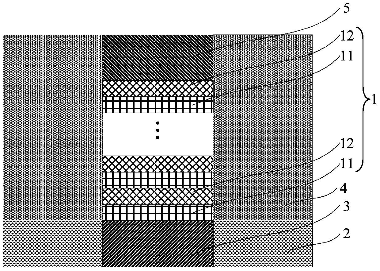
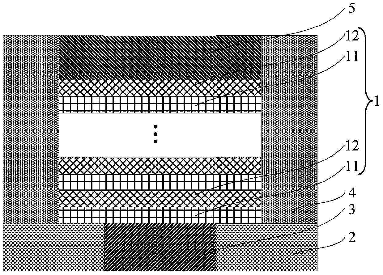
[0068] see figure 2 and image 3 , the present invention also provides a phase-change memory cell, the phase-change memory cell at least includes the phase-change material layer 1 as described in Embodiment 1, that is, the phase-change material layer 1 in this embodiment is the implementation The phase change material layer 1 described in Example 1.

[0069] As an example, the phase change memory unit further includes: a growth substrate 2, a lower electrode 3, a dielectric coating layer 4, and an upper electrode 5; the lower electrode 3 is located in the growth substrate 2 and runs through the growth Substrate 2; the phase-change material layer 1 is located on the surface of the growth substrate 2 and directly above the lower electrode 3; the upper electrode 5 is located on the surface of the phase-change material layer 1; the dielectric coating Layer 4 is located on the surface of the growth substrate 2 and covers the periphery of the phase change material layer 1 and the...

Embodiment 3

[0082] Please combine Figure 6 refer to Figure 7 to Figure 9 , taking the preparation method of a phase-change memory cell with a restricted structure as an example, the preparation method includes the following steps:

[0083] S1: providing a growth substrate 2, wherein a lower electrode 3 is formed in the growth substrate 2, and the lower electrode 3 penetrates the growth substrate 2;

[0084] S2: forming the dielectric cladding layer 4 on the surface of the growth substrate 2;

[0085] S3: forming a first deposition hole 41 in the dielectric coating layer 4, the first deposition hole 41 exposing the lower electrode 3;

[0086] S4: sequentially forming the phase change material layer 1 and the upper electrode 5 in the first deposition hole 41 .

[0087] In step S1, see Figure 7 , providing a growth substrate 2 , a lower electrode 3 is formed in the growth substrate 2 , and the lower electrode 3 penetrates through the growth substrate 2 .

[0088] As an example, the g...


PUM

PropertyMeasurementUnit
thicknessaaaaaaaaaa
thicknessaaaaaaaaaa
thicknessaaaaaaaaaa

Abstract

The invention provides a phase-change material layer, a phase-change memory unit and a preparation method thereof, the phase-change material layer comprising Ti x Te 1‑x layer and located on the Ti x Te 1‑x The Sb layer on the surface of the layer, where 0.33≤x≤0.56. The preparation process of the phase-change material layer in the phase-change memory unit of the present invention is compatible with the existing CMOS process, and has the following advantages: the Sb layer in the selected interval has a very fast phase-change speed so that the phase-change memory has a picosecond The erasing and writing operation time of the level improves the operation speed of the phase change memory; the selected interval Ti x Te 1‑x layer, which can still maintain the stability of the structure at high temperature and improve the thermal stability of the superlattice structure as a whole; Ti x Te 1‑x The layer has better adhesion to the substrate layer, which can increase the number of cycle operations of the device unit and prolong the life of the device unit.

Description

technical field [0001] The invention belongs to the field of semiconductor material preparation, in particular to a phase-change material layer, a phase-change memory unit and a preparation method thereof. Background technique [0002] Memory is an important part of the current semiconductor market and the cornerstone of information technology, playing an important role in both life and the national economy. With the rapid increase of the amount of information along with social development, the research and development of memory with high data storage density has become an important task for memory researchers. Among them, the phase-change memory unit is considered by the International Semiconductor Industry Association to be the most likely to be replaced due to its advantages such as high-speed reading, high erasable times, non-volatility, small component size, low power consumption, strong vibration resistance and radiation resistance. The current flash memory becomes th...

Claims


Application Information

Patent Timeline
Patent Type & Authority Patents(China)
IPC IPC(8): H01L45/00
CPCH10N70/011H10N70/8828
Inventor 宋志棠丁科元饶峰
Owner SHANGHAI INST OF MICROSYSTEM & INFORMATION TECH CHINESE ACAD OF SCI
Why Eureka
Try Eureka