Nanometer composite multilayer phase-change film and preparation method and application thereof

A nano-composite and thin-film technology, applied in the field of microelectronic materials, can solve the problems of slow phase transition speed, low crystallization speed, and inability to meet, and achieve the effects of reducing operating power consumption, improving heating efficiency, and reducing thermal conductivity.

Inactive Publication Date: 2017-06-09
TONGJI UNIV
View PDF6 Cites 5 Cited by
  • Summary
  • Abstract
  • Description
  • Claims
  • Application Information

AI Technical Summary

Problems solved by technology

Nevertheless, Ge 2 Sb 2 Te 5 There are still many problems to be improved in phase change materials: first, Ge 2 Sb 2 Te 5 The performance indicators of phase change materials such as crystallization temperature (160°C), crystallization activation energy (2.24eV) and ten-year data retention (85°C) cannot meet the requirements of automotive electronics (120°C) and aviation (150°C); Two, Ge 2 Sb 2 Te 5 The crystallization mechanism of phase change materials belongs to the nucleation dominant type, and the slow phase change speed cannot meet the requirements of future high-speed memories; thirdly, Ge 2 Sb 2 Te 5 The large density change ratio (6.8%) of phase change materials before and after phase change greatly reduces the reliability and fatigue characteristics of PCM
The selected binary phase change material Ge in the present invention 50 Te 50 It has the advantages of high crystallization temperature and good thermal stability, but its crystallization speed is relatively low and the high and low resistance switch ratio is large; the Sb-rich binary phase change material Ge 8 Sb 92 It has a fast crystallization speed, which can realize high-speed data storage, but its low crystallization temperature is not conducive to the stability and reliability of data storage, and the low crystal resistance leads to relatively high operating power consumption

Method used


Image

  • Nanometer composite multilayer phase-change film and preparation method and application thereof
  • Nanometer composite multilayer phase-change film and preparation method and application thereof
  • Nanometer composite multilayer phase-change film and preparation method and application thereof

Examples


Embodiment 1

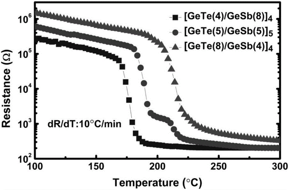
[0035] Ge prepared in this implementation 50 Te 50 / Ge 8 Sb 92 Nanocomposite multilayer phase change film, the total thickness is about 50nm, the general structure is [Ge 50 Te 50 (a) / Ge 8 Sb 92 (b)] x , Where a is Ge in a single cycle 50 Te 50 The thickness of the film, b is Ge in a single cycle 8 Sb 92 The thickness of the film, x is the total period of the nanocomposite multilayer phase change film, the specific structure is [Ge 50 Te 50 (4nm) / Ge 8 Sb 92 (8nm)) 4 .

[0036] 1. Cleaning SiO 2 / Si(100) substrate surface and back, to remove dust particles, organic and inorganic impurities:

[0037] (a) Place the substrate in an ethanol solution and clean it with ultrasonic for 20 minutes to remove dust particles and inorganic impurities on the surface of the substrate;

[0038] (b) Put the substrate in an acetone solution and clean it with ultrasonic for 20 minutes to remove organic impurities on the surface of the substrate;

[0039] (c) Put the substrate in deionized water, clean it ...

Embodiment 2

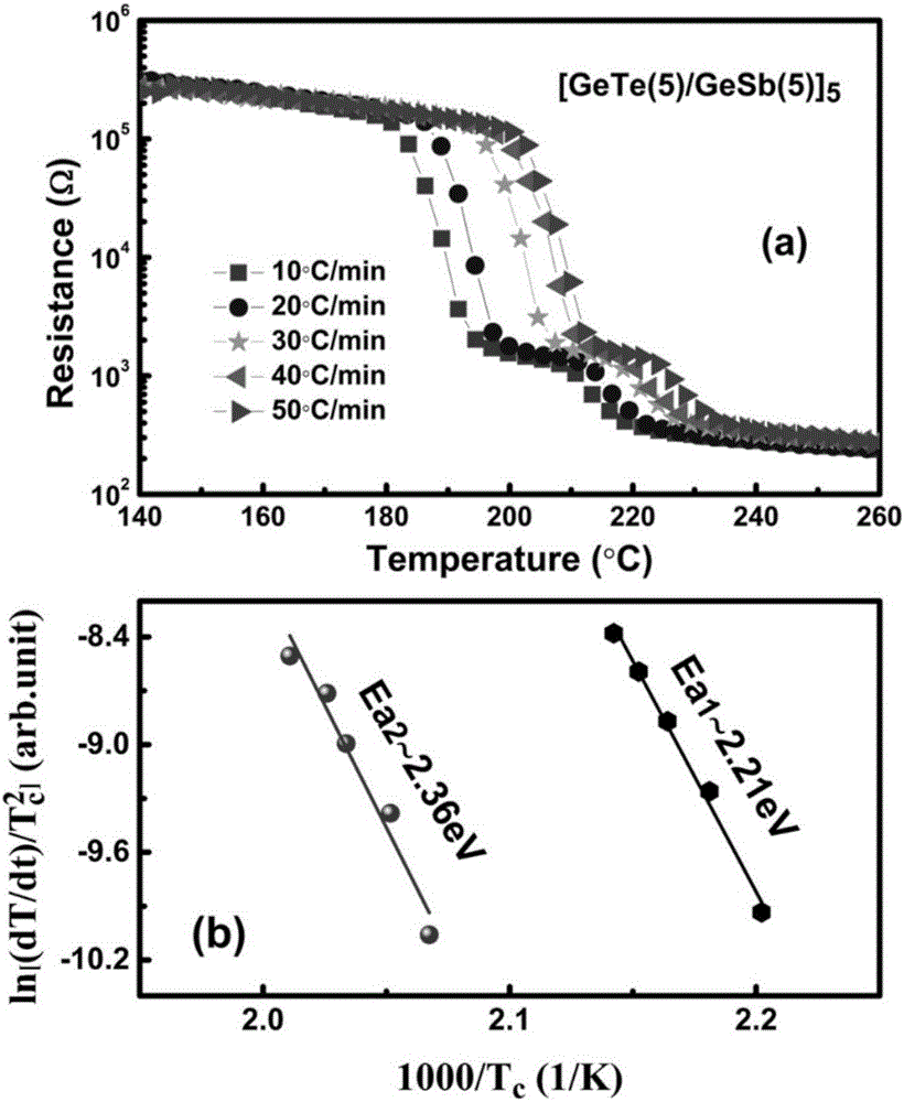
[0051] A nano-composite multilayer phase change film, the preparation method adopted is roughly the same as that of Example 1, except that the specific structure of the nano-composite multilayer phase change film prepared by this embodiment is [Ge 50 Te 50 (5nm) / Ge 8 Sb 92 (5nm)) 5 .

Embodiment 3

[0053] A nano-composite multilayer phase change film, the preparation method adopted is roughly the same as that of Example 1, except that the specific structure of the nano-composite multilayer phase change film prepared by this embodiment is [Ge 50 Te 50 (8nm) / Ge 8 Sb 92 (4nm)) 4 .

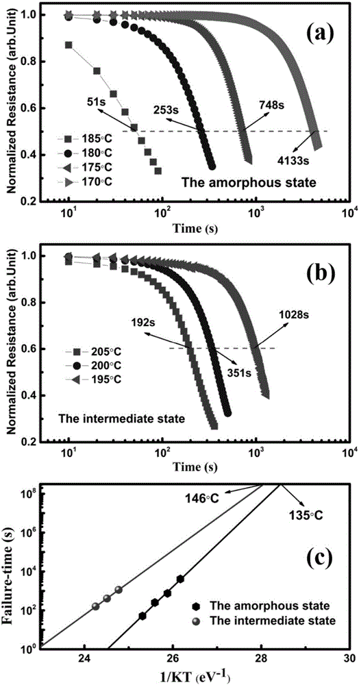
[0054] The Ge of the above embodiment 50 Te 50 / Ge 8 Sb 92 Nanocomposite multilayer phase change film materials are tested, and the in-situ resistance and temperature curves of each phase change film material are obtained, such as figure 1 Shown; the [Ge 50 Te 50 (5nm) / Ge 8 Sb 92 (5nm)) 5 The nanocomposite multilayer phase change film was tested, and the Kissinger equation was used to fit [Ge 50 Te 50 (5nm) / Ge 8 Sb 92 (5nm)) 5 The crystallization activation energy corresponding to the first phase transition and the second phase transition of the film, such as figure 2 Shown; the [Ge 50 Te 50 (5nm) / Ge 8 Sb 92 (5nm)) 5 The nanocomposite multilayer phase change film is tested, and the Arrhenius equation...


PUM

PropertyMeasurementUnit
Total thicknessaaaaaaaaaa

Abstract

The present invention relates to a nanometer composite multilayer phase-change film and a preparation method and an application thereof. The phase-change film is obtained by sputtering a Ge50Te50 phase-change material and a Ge8Sb92 phase-change material periodically, and when the phase-change film is prepared, a SiO2 / Si(100) substrate is cleaned, a sputtering target material is installed, a mechanical pump and a molecular pump are turned on orderly to vacuumize, the flow of a sputtering gas, the sputtering air pressure in a cavity and the sputtering power of the target material are set, and a room temperature magnetic control sputtering method is adopted to prepare the [Ge50Te50(a) / Ge8Sb92(b)]x nanometer composite multilayer phase-change film. Compared with the prior art, the nanometer composite multilayer phase-change film of the present invention has the advantages of good heat stability, fast phase-change speed, high storage density, etc.

Description

Technical field [0001] The invention belongs to the technical field of microelectronic materials, and in particular relates to a nano-composite multilayer phase change film and a preparation method and application thereof. Background technique [0002] Phase change memory (PCM) is a new type of non-volatile semiconductor memory. Its principle is to use phase change materials to switch between high-resistance amorphous state and low-resistance polycrystalline state under the action of electric pulse heating. High-speed reversible transformation to realize binary information storage. PCM write operation (RESET) refers to applying a short and strong electric pulse to the phase change material to raise the temperature of the phase change material to the melting temperature (T m ) Above, and after rapid quenching, the long-range order of the crystalline state of the material is destroyed, and the material is transformed from the crystalline state to the amorphous state. The PCM wipe ...

Claims


Application Information

Patent Timeline
IPC IPC(8): H01L45/00B82Y30/00
CPCB82Y30/00H10N70/881H10N70/8828H10N70/026
Inventor 翟继卫吴卫华陈施谕
Owner TONGJI UNIV
Why Eureka
Try Eureka