
Switching circuit and power supply circuit provided therewith

A technology of switching circuits and power circuits, applied in circuits, electronic switches, high-efficiency power electronic conversion, etc., can solve problems such as difficult operation, damage to power transistors, and large current flow, so as to prevent damage and prevent surges Effect

Active Publication Date: 2017-05-10
SHARP KK
View PDF7 Cites 8 Cited by
  • Summary
  • Abstract
  • Description
  • Claims
  • Application Information

AI Technical Summary

Problems solved by technology

Therefore, when a drain voltage is applied instead of a sufficient negative polarity voltage to the gate terminal of the power transistor, a large current may flow, and the power transistor may be destroyed.
Therefore, power transistors are more difficult to handle than normally-off transistors such as bipolar transistors and Metal Oxide Semiconductor Field Effect Transistors (MOSFETs).

Method used


Image

  • Switching circuit and power supply circuit provided therewith
  • Switching circuit and power supply circuit provided therewith
  • Switching circuit and power supply circuit provided therewith

Examples


no. 1 Embodiment approach

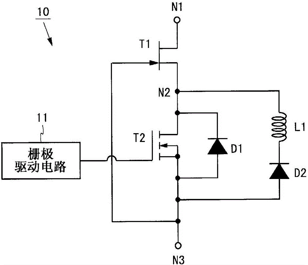
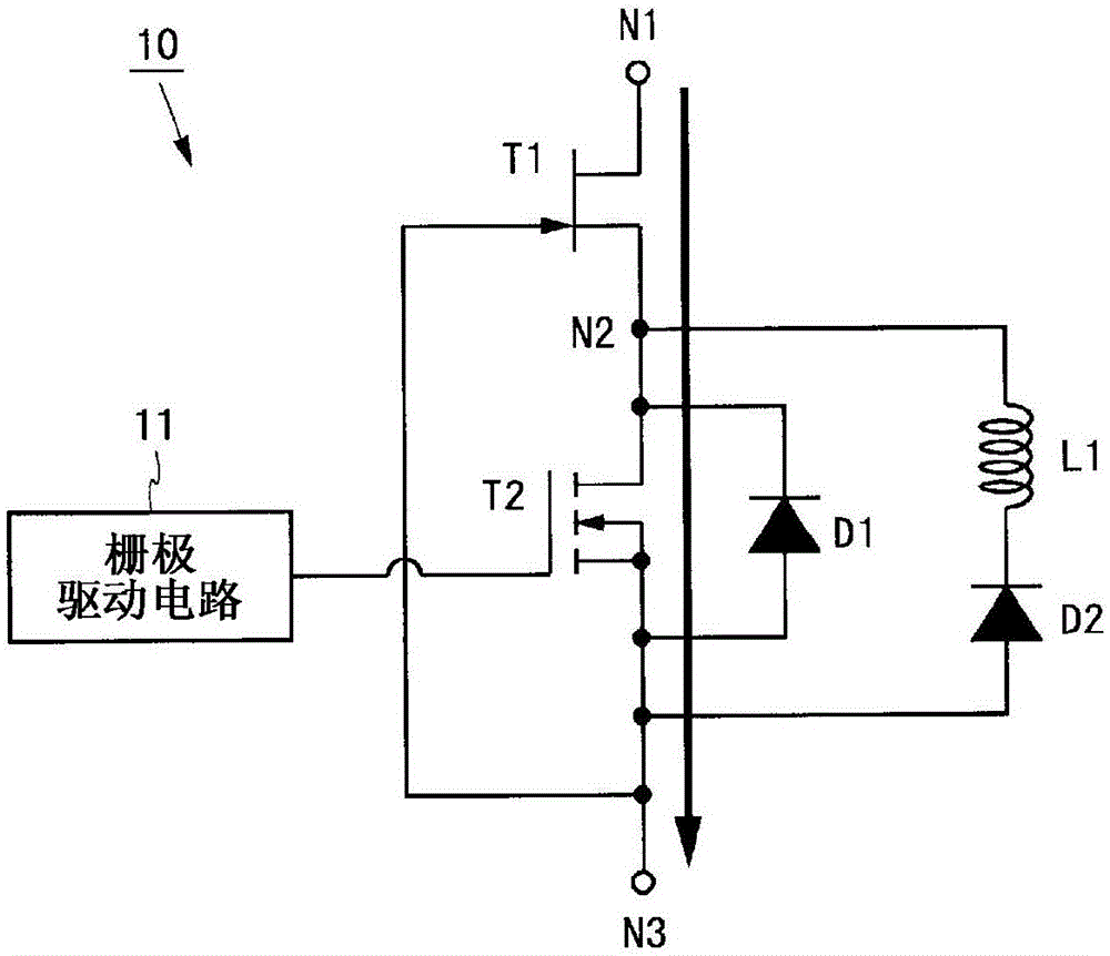
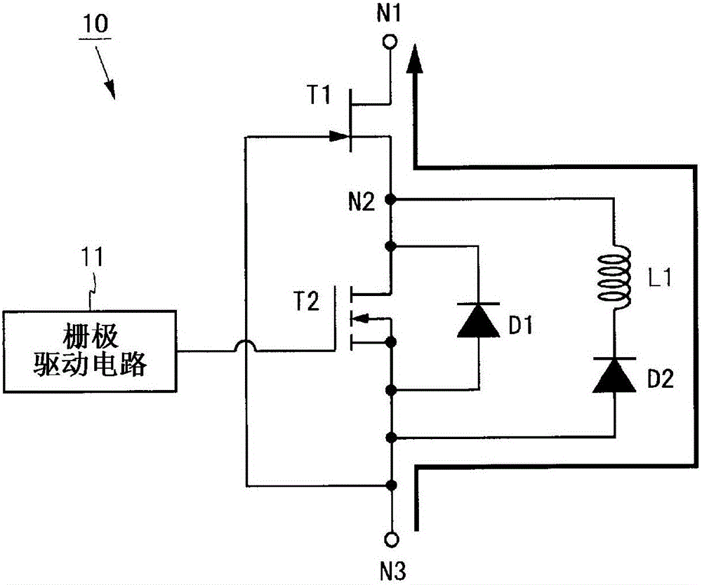
[0095] figure 1 It is a circuit diagram of the switch circuit of 1st Embodiment of this invention. figure 1 The illustrated switch circuit 10 includes transistors T1 , T2 , diodes D1 , D2 , and a gate drive circuit 11 . The switch circuit 10 has a high withstand voltage normally-on transistor and a low withstand voltage normally-off transistor connected in series.

[0096] exist figure 1 Among them, the transistor T1 is an N-channel and high withstand voltage normally-on transistor. The transistor T2 is an N-channel, low-voltage normally-off transistor. Diode D1 is a PN junction diode. As the diode D1, for example, a built-in diode (also called a parasitic diode) of the transistor T2 is used. Diode D2 has a lower forward voltage than diode D1. For the diode D2, for example, a Schottky barrier diode is used. Thus, in the switch circuit 10, the breakdown voltage of the transistor T1 is higher than the breakdown voltage of the transistor T2, and the forward voltage of t...

no. 2 Embodiment approach

[0119] Figure 5 It is a circuit diagram of the switch circuit of 2nd Embodiment of this invention. Figure 5 The illustrated switch circuit 20 includes transistors T2 , T4 , diodes D1 , D2 , D4 , and D5 , a gate drive circuit 11 , and a gate power supply circuit 21 . The switch circuit 20 has two normally-off transistors connected in series. In the following description, among the constituent elements of each embodiment, the same reference numerals are attached to the same elements as those in the above-described embodiment, and description thereof will be omitted.

[0120] exist Figure 5 Among them, the transistor T4 is an N-channel and high withstand voltage normally-off MOSFET. Diode D4 is a built-in diode of transistor T4. The diode D5 is a Zener diode provided to protect the transistor T2. As the diode D2, a diode having a forward voltage lower than that of the diodes D1 and D5 is used. In addition, the switch circuit 20 does not have to include the diode D5. Thu...

no. 3 Embodiment approach

[0139] Figure 7 It is a circuit diagram of the power supply circuit of 3rd Embodiment of this invention. Figure 7 The illustrated power supply circuit 30 is a step-up chopper circuit including a switch circuit 10 , a transistor T3 , a diode D3 , a gate drive circuit 31 , a coil L0 , and capacitors C1 and C2 . exist Figure 7 , the power supply circuit 30 is connected to a power supply 1 and a load R1. The capacitor C1 is arranged in parallel with the power supply 1, and the capacitor C2 is arranged in parallel with the resistor R1. In addition, the power supply circuit 30 does not need to include the capacitors C1 and C2.

[0140] The switch circuit 10 is the circuit described in the first embodiment. The transistor T3 is an N-channel normally-off transistor. Diode D3 is arranged in antiparallel with transistor T3. The cathode terminal of diode D3 is connected to the drain terminal of transistor T3, and the anode terminal of diode D3 is connected to the source terminal...


PUM


Abstract

A high-withstand-voltage normally-on transistor (T1) and a low-withstand-voltage normally-off transistor (T1) are connected in series, and diodes (D1,D2) are provided in reverse parallel to the transistor (T2). A gate terminal of the transistor (T1) is connected to a source terminal of the transistor (T2), and a gate driving circuit (11) that outputs a control signal to a gate terminal of the transistor (T2) is provided. Forward voltage of the diode (D2) is made lower than forward voltage of the diode (D1), and an inductance component of a path connecting nodes (N1) (N3)via the diode (D1) is made greater than an inductance component of a path connecting the nodes (N2) (N3) via the diode (D1). Accordingly, a switching circuit which includes transistors connected in series and in which transient current at a time of turning off is reduced is provided.

Description

technical field [0001] The present invention relates to a switching circuit and a power supply circuit, and more particularly to a switching circuit including transistors connected in series and a power supply circuit including the switching circuit. Background technique [0002] Power transistors generally have a normally-on characteristic in which a drain current flows when the gate-source voltage is 0V. Therefore, when a drain voltage is applied instead of a sufficient negative polarity voltage to the gate terminal of the power transistor, a large current flows, and the power transistor may be destroyed. Therefore, power transistors are more difficult to handle than normally-off transistors such as bipolar transistors and Metal Oxide Semiconductor Field Effect Transistors (MOSFETs). [0003] Therefore, conventionally, there is known a switch circuit in which a high breakdown voltage normally-on transistor and a low breakdown voltage normally-off transistor are connected ...

Claims


Application Information

Patent Timeline
Patent Type & Authority Applications(China)
IPC IPC(8): H03K17/16H02M3/155H03K17/10H03K17/695
CPCH02M1/08H02M3/1588H03K17/08142H03K17/102H03K17/162H03K2017/6875Y02B70/10H02M1/346H02M3/1555H02M3/158H03K17/08
Inventor 片冈耕太郎盐见竹史若生周治五十岚弘树柴田晃秀岩田浩
Owner SHARP KK
Learn More