Energy-saving and environment-friendly solder tip and production process thereof

An energy-saving, environmental-friendly, production-technical technology, applied in soldering irons, manufacturing tools, metal processing equipment, etc., can solve problems such as large thickness deviation of iron plating layer, long production cycle, wrong operation, etc. Electroplating wastewater, the effect of improving the service life

Inactive Publication Date: 2017-05-17
深圳市吉美电子设备有限公司
View PDF5 Cites 5 Cited by
  • Summary
  • Abstract
  • Description
  • Claims
  • Application Information

AI Technical Summary

Problems solved by technology

When the soldering iron tip is soldering, the tin liquid will continuously corrode the electroplated iron layer at a normal speed at high temperature, but when the high-temperature tin liquid encounters the pores and bubbles in the electroplating, the high-temperature tin liquid will accelerate to the electroplated iron layer through the pores or bubbles. The internal corrosion of the iron layer greatly reduces the service life of the soldering iron tip; at the same time, the size and position of the pores and bubbles are randomly distributed in the iron layer, resulting in different service life of the produced soldering iron tip;
[0005] 2. In the existing electroplating process, the high-temperature steam of the electroplating solution will volatilize seriously, endangering human health; and it will discharge a large amount of electroplating sewage, causing environmental pollution;
[0006] 3. The existing soldering iron tip production process needs to go through processes such as cutting copper blanks, copper blank polishing, cleaning, and iron plating. The entire process takes more than 480 minutes. The production cycle is long and the cost is high; at the same time, artificial processing is required Constantly adjust the thickness of the iron plating layer by judgment, the quality of the finished product is very dependent on the experience of the workers, and the degree of automation is not high;
[0007] 4. For the soldering iron tip produced by the existing technology of the iron plating layer on the outer copper embryo, the copper embryo and the electroplating iron layer are wrapped inside and outside. Because the electroplating layer is too thick, the workpiece is deformed irregularly, resulting in the copper embryo and the iron plating layer The concentricity deviation is very large. After the turning process, the thickness deviation around the iron plating layer wrapped around the copper embryo is relatively large. In this way, when the soldering iron tip is soldering, although the thick iron layer is not damaged, the iron layer The thin part will be corroded by the high-temperature tin liquid to the inner copper germ layer first, so that the perforation of the soldering iron tip will not work normally, which will also make the life of the soldering iron tip different, and the quality is very unstable
[0008] 5. The soldering iron tip produced by the existing technology of electroplating the iron layer outside the copper embryo will be electroplated with a layer of decorative chrome after the electroplated iron layer is trimmed. Due to the limitation of the process, the thickness of the decorative chrome will not exceed 0.08mm Time prevents the corrosion of the tin liquid. During the use of the soldering iron tip, the tin liquid will run upwards outside the working area, which will cause incorrect operation.
Because the iron layer above the working area is getting thinner and thinner, the tin liquid will continue to corrode these iron layers until it corrodes the copper embryo layer below the iron layer, so that the perforation of the soldering iron tip cannot work normally, which will also make the life of the soldering iron tip vary. , the quality is very unstable
[0009] Due to the existence of these defects, the production, use and promotion of soldering iron tips are limited, and the formulation of highly standardized production process standards is also limited.

Method used


Image

  • Energy-saving and environment-friendly solder tip and production process thereof
  • Energy-saving and environment-friendly solder tip and production process thereof
  • Energy-saving and environment-friendly solder tip and production process thereof

Examples


Embodiment Construction

[0043] In order to express the present invention more clearly, the present invention will be further described below in conjunction with the accompanying drawings.

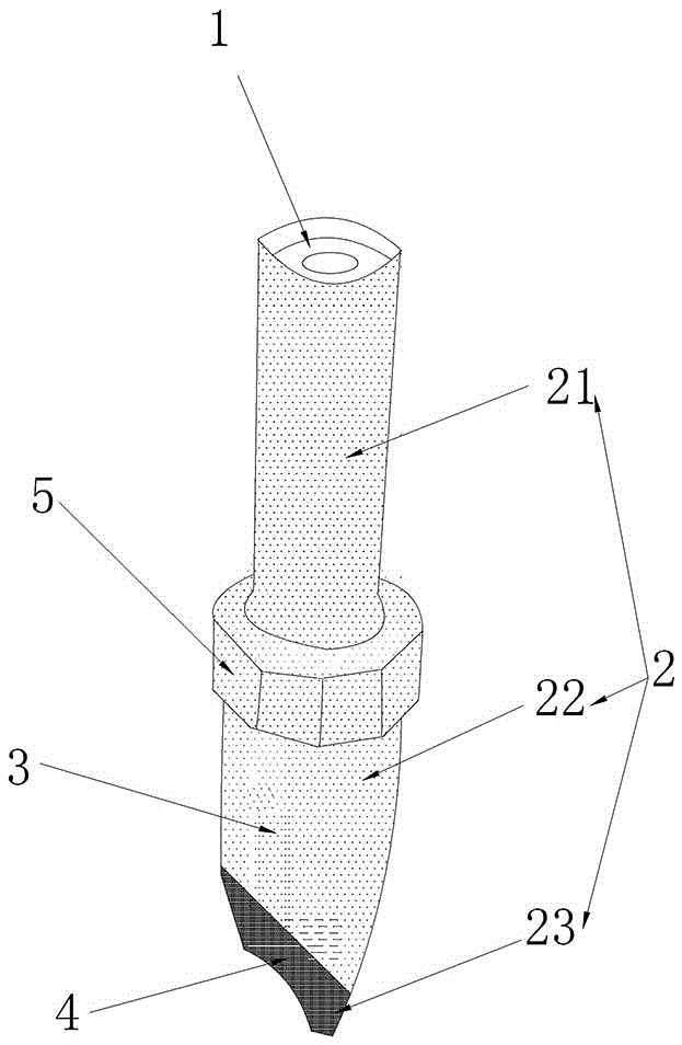
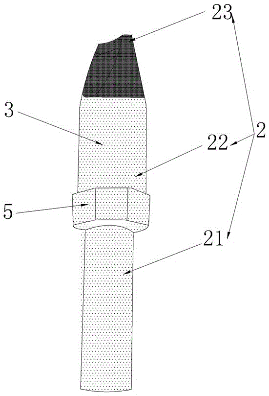
[0044] see Figure 1-2 , the energy-saving and environment-friendly soldering iron tip provided by the present invention and its production process include a copper embryo 1 for connecting with a soldering iron core, an iron embryo 2 for slowing down tin corrosion, a tin layer 4 and an anti-corrosion metal layer 3 that is not easily corroded by tin, The iron embryo 2 includes a first embryo body 21 and a second embryo body 22, the first embryo body 21 and the second embryo body 22 are integrally formed, and the first embryo body 21 is provided with a copper embryo groove for fixing and accommodating the copper embryo 1. The second blank body 22 is provided with a working end 23 for soldering operation; the anti-corrosion metal layer 3 is sprayed and covered on the outer surface of the first blank body 21 and the s...


PUM

PropertyMeasurementUnit
thicknessaaaaaaaaaa

Abstract

The invention discloses an energy-saving and environment-friendly solder tip and a production process thereof. During production of the solder tip, copper billet manufacturing, iron billet manufacturing, copper billet and iron billet combination, shape processing, surface polishing, spraying of an anti-corrosion metal layer, hot galvanizing of a molten tin protection layer and the like are sequentially conducted to finally form a copper billet, an iron billet, the anti-corrosion metal layer and a tin layer, wherein the iron billet comprises a first billet body and a second billet body which are integrally formed; a copper billet groove for fixing and accommodating the copper billet is formed in the first billet body; a working end for tin soldering operation is arranged at the second billet body; the anti-corrosion metal layer is sprayed to cover the outer surface of the second billet body; and the tin layer covers a solder tip on the outer surface of the working end. The process is simple, the cost is low, the environment is protected, a produced product is stable in performance, the production period is short, and automatic production can be realized.

Description

technical field [0001] The invention relates to the field of mechanical products, in particular to an energy-saving and environment-friendly soldering iron tip and a production process thereof. Background technique [0002] With the development of the economic era, electronic technology and electronic components occupy an increasingly important position in society, among which soldering iron tips are very important in the processing of electronic products. [0003] The existing soldering iron tip mainly adopts the method of copper outer iron plating in the processing process, that is, the iron layer is electroplated on the outer layer of the existing copper embryo. This method will have the following defects: [0004] 1. During the electroplating process, a large number of pores and bubbles will be generated in the iron layer. The size and position of these pores and bubbles are randomly distributed in the iron layer. When the soldering iron tip is soldering, the tin liquid...

Claims


Application Information

Patent Timeline
Patent Type & Authority Applications(China)
IPC IPC(8): B23K3/02B23P15/00
CPCB23K3/025B23P15/00
Inventor 陈芝明贺蓉
Owner 深圳市吉美电子设备有限公司
Why Eureka
Try Eureka