Two-dimensional material flexible substrate structure, semiconductor light emitting device and manufacturing method thereof

A flexible substrate and two-dimensional material technology, applied in the semiconductor field, can solve the problem that the flexible substrate cannot fully absorb and release stress, and achieve the effects of increasing device integration functions, reducing costs, and expanding wavelengths

Inactive Publication Date: 2017-05-17
CHAOJING TECH BEIJING CO LTD
View PDF4 Cites 9 Cited by
  • Summary
  • Abstract
  • Description
  • Claims
  • Application Information

AI Technical Summary

Problems solved by technology

[0004] In view of the shortcomings of the prior art described above, the purpose of the present invention is to provide a two-dimensional material flexible substrate structure, a semiconductor light-emitting device and its manufacturing method, which are used to solve the problem that the flexible substrate in the prior art cannot completely absorb and release stress problem

Method used


Image

  • Two-dimensional material flexible substrate structure, semiconductor light emitting device and manufacturing method thereof
  • Two-dimensional material flexible substrate structure, semiconductor light emitting device and manufacturing method thereof
  • Two-dimensional material flexible substrate structure, semiconductor light emitting device and manufacturing method thereof

Examples


Embodiment 1

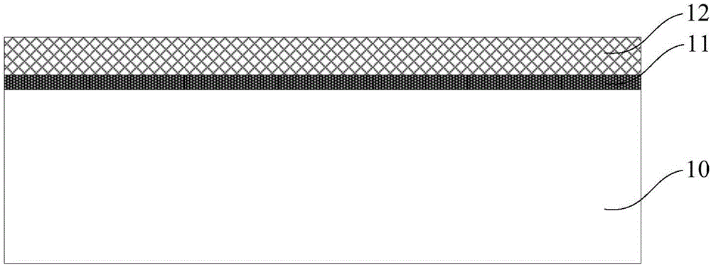
[0071] see figure 1 , the present invention provides a two-dimensional material flexible substrate structure, the two-dimensional material flexible substrate structure includes: a supporting substrate 10; a two-dimensional material layer 11, the two-dimensional material layer 11 is located on the supporting substrate 10 surface; a flexible substrate 12, the flexible substrate 12 is located on the surface of the two-dimensional material layer 11.

[0072] As an example, the supporting substrate 10 may be a semiconductor substrate, a semi-insulator substrate, an insulator substrate, or a thermally conductive material substrate. Preferably, in this embodiment, the supporting substrate 10 is a Si substrate.

[0073] As an example, the two-dimensional material layer 11 may be a graphene layer, a silicene layer, a germanene layer, a BN layer, MoS 2 Layer or WS 2 layer. Preferably, in this embodiment, the two-dimensional material layer 11 is a graphene layer.

[0074] As an exam...

Embodiment 2

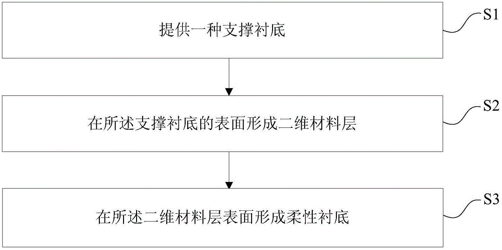
[0078] see figure 2 , the present invention also provides a method for manufacturing a two-dimensional material flexible substrate structure, the method for manufacturing a two-dimensional material flexible substrate structure includes the following steps:

[0079] 1) providing a support substrate;

[0080] 2) forming a two-dimensional material layer on the surface of the supporting substrate;

[0081] 3) Forming a flexible substrate on the surface of the two-dimensional material layer.

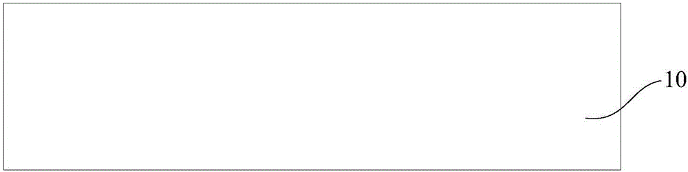
[0082] To perform step 1), see figure 2 Step S1 in and image 3 , providing a support substrate 10 .

[0083] As an example, the supporting substrate 10 may be a semiconductor substrate, a semi-insulator substrate, an insulator substrate, or a thermally conductive material substrate. Preferably, in this embodiment, the supporting substrate 10 is a Si substrate.

[0084] Execute step 2), see figure 2 Step S2 in and Figure 4 , forming a two-dimensional material layer 11 on the surfa...

Embodiment 3

[0100] see Figure 11 and Figure 12, the present invention also provides a semiconductor light emitting device, the semiconductor light emitting device includes: the two-dimensional material flexible substrate structure described in Embodiment 1 and a light emitting device material layer 17, the light emitting device material layer 17 is located on the flexible the surface of the substrate. For the specific structure of the two-dimensional material flexible substrate structure, please refer to Embodiment 1, which will not be repeated here.

[0101] see Figure 11 , in an example, the light emitting device material layer includes: a lower electrode 171, the lower electrode 171 is located on the surface of the flexible substrate 12; a lower waveguide layer 172, the lower waveguide layer 172 is located on the lower electrode 171 The surface of the quantum well layer 173, the quantum well layer 173 is located on the surface of the lower waveguide layer 172, and the quantum wel...


PUM

PropertyMeasurementUnit
thicknessaaaaaaaaaa
thicknessaaaaaaaaaa
thicknessaaaaaaaaaa

Abstract

The invention provides a two-dimensional material flexible substrate structure, and a semiconductor light emitting device and a manufacturing method thereof. The two-dimensional material flexible substrate structure comprises a support substrate, a two-dimensional material layer positioned on the surface of the support substrate, and a flexible substrate positioned on the surface of the two-dimensional material layer. According to the two-dimensional material flexible substrate structure provided by the invention, the flexible substrate is combined with the two-dimensional material layer, attraction between upper and lower atoms is greatly weakened by Van der Waals bonding at an interface between the flexible substrate and the two-dimensional material, strength of a Van der Waals force formed at the interface is far less than bond energy of a covalent bond, the flexible substrate can completely self-control strain absorption and release stress, and has extremely high absolute flexibility; the semiconductor light emitting device based on the two-dimensional material flexible substrate structure provided by the invention has the advantages of expanding wavelength, reducing cost, promoting heat dissipation, improving service life of the device and increasing integrated functions of the device.

Description

technical field [0001] The invention belongs to the technical field of semiconductors, and relates to a two-dimensional material flexible substrate structure, a semiconductor light-emitting device and a manufacturing method thereof. Background technique [0002] Semiconductor light-emitting devices include light-emitting diodes (Light Emitting Diode, LED) and various types of semiconductor lasers (Laser Diode, LD), because of their small size, low power consumption, high quantum conversion efficiency, long life and other advantages, they are widely used in lighting, communication , industrial processing, medicine and many fields in daily life, its wavelength range covers ultraviolet, visible light, short-wave, medium-wave and long-wave infrared, and finally to the terahertz band. Commercial semiconductor light-emitting devices are limited by the substrate, so they can only design device structures and perform epitaxial growth on limited types of substrates such as silicon, s...

Claims


Application Information

Patent Timeline
Patent Type & Authority Applications(China)
IPC IPC(8): H01S5/02
CPCH01S5/0206
Inventor 王庶民
Owner CHAOJING TECH BEIJING CO LTD
Why Eureka
Try Eureka