QLED field effect transistor with improved light extraction ratio, and preparation method for QLED field effect transistor

A field-effect transistor and light extraction rate technology, which is used in semiconductor/solid-state device manufacturing, photovoltaic power generation, electric solid-state devices, etc., can solve the problems of low light extraction rate of integrated light-emitting devices, etc. Effect

Inactive Publication Date: 2017-05-24
TCL CORPORATION
View PDF3 Cites 8 Cited by
  • Summary
  • Abstract
  • Description
  • Claims
  • Application Information

AI Technical Summary

Problems solved by technology

[0005] In view of the above-mentioned deficiencies in the prior art, the object of the present invention is to provide a QLED field-effect transistor with enhanced

Method used


Image

  • QLED field effect transistor with improved light extraction ratio, and preparation method for QLED field effect transistor
  • QLED field effect transistor with improved light extraction ratio, and preparation method for QLED field effect transistor
  • QLED field effect transistor with improved light extraction ratio, and preparation method for QLED field effect transistor

Examples


Embodiment 1

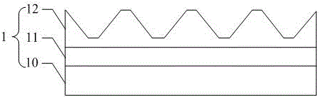
[0041] Such as image 3 As shown, the SOI substrate is cleaned by the standard Shiraki method, including organic solvent ambient ultrasonic, multi-step strong acid treatment, etc. to remove the surface insulating layer and organic impurities and metal element impurities. The SOI substrate sequentially includes a first silicon layer 30 , an insulating layer 31 and a second silicon layer 32 from bottom to top.

[0042] The first silicon layer 30 can be N-type doped, the first silicon layer 30 is used as the first electrode, the first electrode is the cathode of the FET, and the gate of the FET at the same time.

[0043] The insulating layer 31 can choose PMMA or polyimide (PI) material. For example, when choosing PI material, PI and N,N-dimethylformamide (DMF) can be diluted at a volume ratio of 1:1 and spin coated on the first silicon layer 30. Then dry in an infrared box for 5 minutes, and then anneal for 3 hours in an argon atmosphere at 220°C.

[0044] Etching is performe...

Embodiment 2

[0050] Such as Figure 4 As shown, the SOI substrate is cleaned by the standard Shiraki method, including organic solvent ambient ultrasonic, multi-step strong acid treatment, etc. to remove the surface insulating layer and organic impurities and metal element impurities. The SOI substrate includes a first silicon layer 40 , an insulating layer 41 and a second silicon layer 42 sequentially from bottom to top.

[0051] The first silicon layer 40 can be N-type doped, the first silicon layer 40 is used as the first electrode, and the first electrode is the anode of the FET and also the gate of the FET.

[0052] The insulating layer 41 can be made of PMMA or polyimide (PI). For example, when choosing PI material, PI and N,N-dimethylformamide (DMF) can be diluted at a volume ratio of 1:1 and spin coated on the first silicon layer 40. Then dry in an infrared box for 5 minutes, and then anneal for 3 hours in an argon atmosphere at 220°C.

[0053] Etching is performed on the surfac...


PUM

PropertyMeasurementUnit
Thicknessaaaaaaaaaa
Thicknessaaaaaaaaaa
Thicknessaaaaaaaaaa

Abstract

The invention discloses a QLED field effect transistor with the improved light extraction ratio, and a preparation method for the QLED field effect transistor. The QLED field effect transistor sequentially comprises an SOI substrate with the surface being provided with a plurality of nano-pits, and an OLED device located on the surface of the SOI substrate. The SOI substrate comprises a first silicon layer, an insulating layer and a second silicon layer, wherein the first silicon layer, the insulating layer and the second silicon layer are sequentially arranged. According to the invention, the surface of the SOI substrate is provided with the plurality of nano-pits, thereby enabling the surface of the SOI substrate to be in an uneven structure, and enabling the QLED device to form an uneven structure. Compared with a conventional plane structure, the QLED field effect transistor can improve the light extraction ratio, and improve the luminous efficiency of the device.

Description

technical field [0001] The invention relates to the display field, in particular to a QLED field effect transistor with enhanced light extraction rate and a preparation method thereof. Background technique [0002] In recent years, quantum dot light-emitting diodes (QLEDs) have attracted extensive attention and research in the fields of lighting and display due to their advantages such as high brightness, low power consumption, wide color gamut, and easy processing. In addition, in the context of the development of microelectronics technology, field effect transistors (FETs) are currently one of the most widely used devices in modern microelectronics. With the maturity of small size and passive driving technology, large size and active driving technology display has become the mainstream of research, and large size display requires TFT driving technology. By combining the technology of light emitting devices and FETs, QLEDs that integrate QLEDs and FETs can be considered -F...

Claims


Application Information

Patent Timeline
IPC IPC(8): H01L27/32H01L51/00
CPCH10K59/00H10K77/10Y02E10/549Y02P70/50
Inventor 辛征航向超宇李乐张滔张东华
Owner TCL CORPORATION
Why Eureka
Try Eureka