Method for reducing fluorescent powder sedimentation rate of surface mount device

A surface mount device and sedimentation rate technology, applied in the direction of electric solid devices, semiconductor devices, electrical components, etc., can solve the problems of wide color range of products, uneven light spots of finished products, and failure to meet the requirements of testing, so as to optimize LED color Concentration, uniform luminous spot, no effect of aperture hole

Inactive Publication Date: 2017-05-24
YLIN ELECTRONICS CO LTD
View PDF4 Cites 0 Cited by
  • Summary
  • Abstract
  • Description
  • Claims
  • Application Information

AI Technical Summary

Problems solved by technology

[0003] However, the current SMD ordinary white light models need to use fluorescent powder to achieve the white light effect. Requirements for tolerance SDCM less than 6
At the same time, the problem of phosphor sedimentation will also affect the optical consistency of LED

Method used


Image

  • Method for reducing fluorescent powder sedimentation rate of surface mount device
  • Method for reducing fluorescent powder sedimentation rate of surface mount device
  • Method for reducing fluorescent powder sedimentation rate of surface mount device

Examples


Embodiment 1

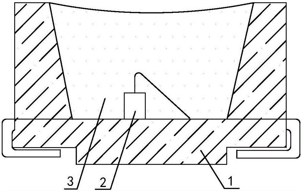
[0030] Such as Figure 1-4 As shown, the method for reducing the sedimentation rate of phosphor powder in the surface mount device described in the embodiment of the present invention mainly consists of the following steps:

[0031] (1) At first, install the light-emitting chip 2 of the built-in chip at the bottom of the SMD support body 1;

[0032] (2) Then, prepare silicone filling glue of model KMT-1212A, colloid of model KMT-1212B, and DM-30 anti-sinking powder. The weight ratio of the three raw materials is 5:0.06:1 in sequence. Mix KMT-1212A silicone filling glue and KMT-1212B colloid and fill it inside the frame to form colloid 5, and there is a descending vertical space with an inverted trapezoidal structure between the top surface of light-emitting chip 2 and colloid 5;

[0033] (3) adding fluorescent powder 3 inside the colloid 5;

[0034] (4) Finally, add the DM-30 anti-sinking powder 4 prepared by step (2) into the colloid 5 obtained in step (3).

Embodiment 2

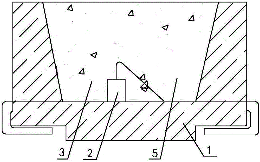
[0036] Such as Figure 1-4 As shown, the method for reducing the sedimentation rate of phosphor powder in the surface mount device described in the embodiment of the present invention mainly consists of the following steps:

[0037] (1) First, arrange the chip at the bottom of the SMD support body 1 and install the light-emitting chip 2, the chip is detachable and has a chip slot inside the SMD support body 1;

[0038] (2) Then, prepare silicone filling glue of model KMT-1212A, colloid of model KMT-1212B, and DM-30 anti-sinking powder. The weight ratio of the three raw materials is 5:0.06:1 in sequence. The silicone filling glue of KMT-1212A and the colloid of model KMT-1212B are mixed and filled inside the frame to form a colloid, and there is a descending vertical space with an inverted isosceles trapezoidal structure between the top surface of the light-emitting chip and the colloid;

[0039] (3) adding fluorescent powder 3 inside the colloid 5;

[0040] (4) Finally, add ...

Embodiment 3

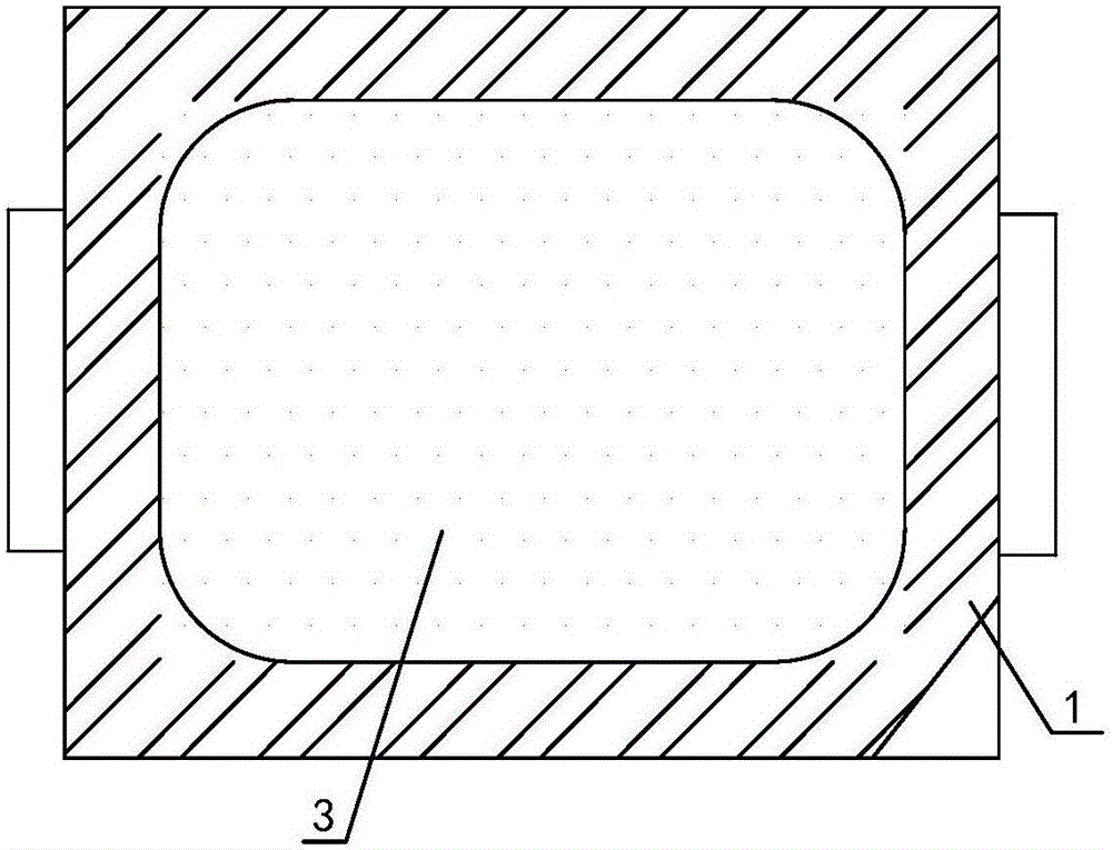
[0042] The method for reducing the sedimentation rate of phosphor powder in the surface mount device described in the embodiment of the present invention, in addition to the steps adopted in embodiment 1 or embodiment 2, also includes that the colloid 5 and the edge of the top surface of the frame A fixed adhesive layer is arranged between the positions; several protruding pin end pieces are formed on the outside of the SMD support body 1 .


PUM


Abstract

The invention relates to a method for reducing a fluorescent powder sedimentation rate of a surface mount device. The method comprises the following steps: taking three raw materials in parts by weight: organosilicone filling glue with the model of KMT-1212A, glue with the model of KMT-1212B and sedimentation-resistant powder of DM-30, wherein a ratio of the three materials is 5:0.06:1, mixing and filling the organosilicone filling glue with the model of KMT-1212A and the glue with the model of KMT-1212B in a rack so as to form colloid; adding fluorescent powder into the colloid; and finally, adding the sedimentation-resistant powder of DM-30 equivalent to 1% of the weight of the colloid into the colloid. The method disclosed by the invention has the beneficial effects that the original fluorescent powder sedimentation rate is reduced, chip light emission is centralized, and light spots are uniform; and by dispensing on the surface of an LED (light-emitting diode) chip in a cup, with the adoption of two kinds of glue with fixed models and the sedimentation-resistant powder of DM-30 with a corresponding ratio, the LED finished product is uniform and full in light emission and light spots, an aperture cavity is avoided, and the LED color concentration ratio is optimized.

Description

technical field [0001] The invention relates to SMD surface mounting LED technology, in particular to a method for reducing the sedimentation rate of fluorescent powder of surface mounting devices used in the fields of toy products, patch LED projection products and the like. Background technique [0002] LED means Surface Mount Light Emitting Diode, SMD patch helps to improve production efficiency and application in different facilities. It is a solid-state semiconductor device that can directly convert electricity into light. Its voltage is 1.9-3.2V, the voltage of red light and yellow light is the lowest. The heart of LED is a semiconductor chip. Epoxy resin encapsulation. Semiconductor wafer is made up of two parts, and a part is P-type semiconductor, and hole occupies an leading position in it, and the other end is N-type semiconductor, and here mainly is electron. When electric current acts on this chip by wire, electron will be pushed to P district, and in P distric...

Claims


Application Information

Patent Timeline
IPC IPC(8): H01L33/48H01L33/54H01L33/56
CPCH01L2224/48091H01L2924/00014H01L33/48H01L33/54H01L33/56H01L2933/0033H01L2933/005
Inventor 林启程
Owner YLIN ELECTRONICS CO LTD
Why Eureka
Try Eureka