

Light-emitting element and method for manufacturing light-emitting element
A technology of a light-emitting element and a manufacturing method, which is applied in the field of its structure, can solve problems such as the inability to manufacture a light-emitting element with a vertical structure, reduce deformation, and cost constraints, and achieve the effects of easy fabrication, suppression of current leakage, and excellent light extraction efficiency
- Summary
- Abstract
- Description
- Claims
- Application Information
AI Technical Summary
Problems solved by technology
Method used
Image

Examples
no. 1 approach >
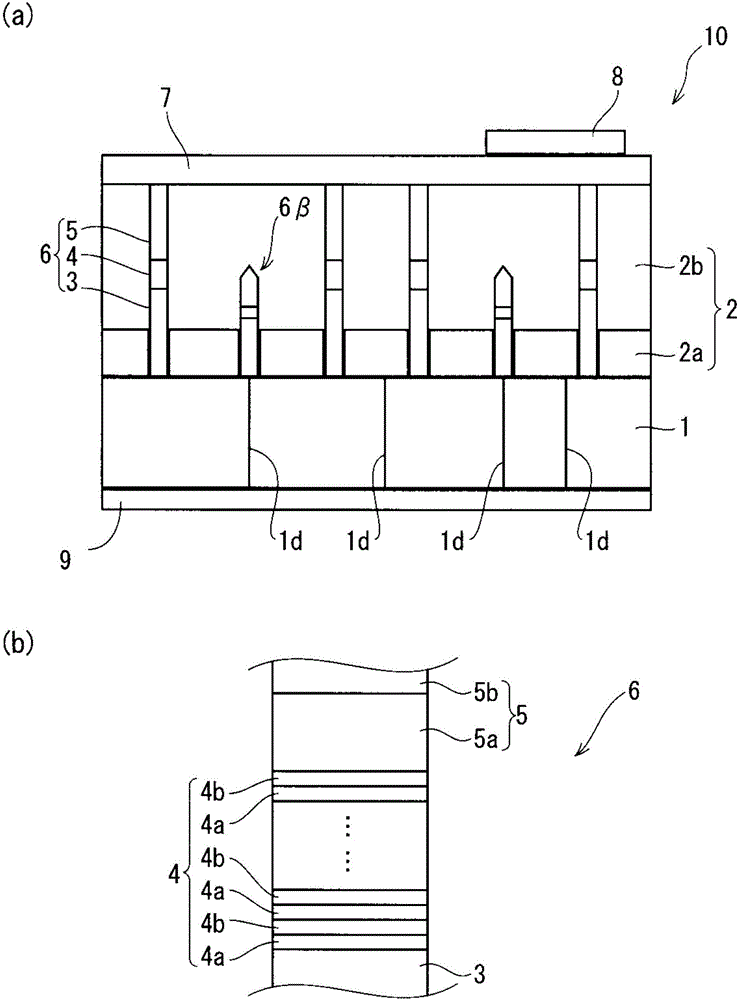
[0048]
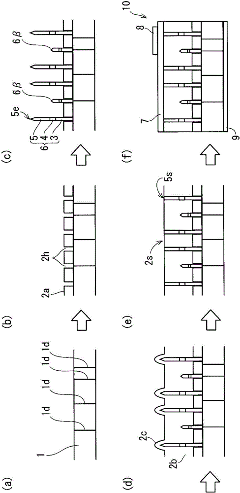
[0049] figure 1 It is a figure which schematically shows the structure of the light emitting element 10 which concerns on this embodiment. figure 1 (a) is a schematic cross-sectional view of the entire light-emitting element 10 . Such as figure 1 As shown in (a), the light-emitting element 10 mainly includes: a base substrate 1, a light confinement layer 2 obtained by sequentially laminating a first light confinement layer 2a and a second light confinement layer 2b from the base substrate side, and a light confinement layer 2 obtained by laminating sequentially from the base substrate side. A plurality of columnar light emitting parts 6 (first columnar structure), transparent conductive film 7, pad electrode 8, and cathode electrode 9. The light emitting element 10 has a substantially vertical light emitting element structure, and when electricity is passed between the pad electrode 8 and the cathode electrode 9, the plurality of columnar light emitting portions ...
no. 2 approach >
[0117]As described above, in the first embodiment (and its modified example), the case where a light-emitting element with a vertical structure excellent in light extraction efficiency is realized by using an aligned polycrystalline substrate, that is, a GaN substrate, as the base substrate 1 has been described. In the embodiment, the light emitting element 210 having a horizontal structure will be described.
[0118] Figure 5 It is a figure which schematically shows the appearance of the light emitting element 210 which concerns on 2nd Embodiment in the manufacturing process. It should be noted that the components included in the light emitting element 210 according to the present embodiment and the same components as those of the light emitting element 10 according to the first embodiment are given the same reference numerals, and detailed description thereof will be omitted. In the following description, the light-emitting element 210 is fabricated by preparing the base s...
Embodiment
[0128] (Example)
[0129] Various light-emitting elements having the same configuration as the light-emitting element 10 according to the first embodiment were fabricated.
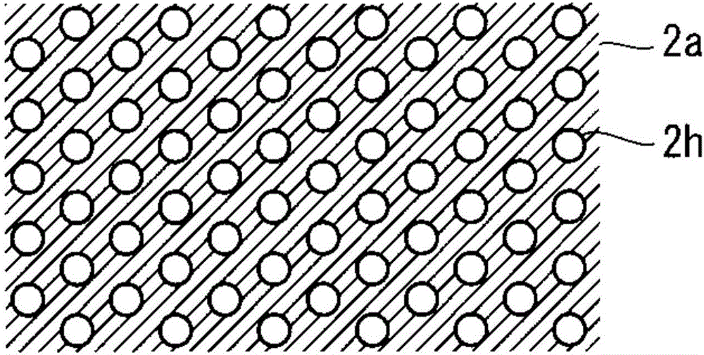
[0130] Specifically, the average particle diameter D in the oriented GaN substrate was varied to three levels of 15 μm, 30 μm, and 50 μm, and the opening diameter (maximum outer diameter dimension of the columnar light emitting portion 6 ) d of the opening 2 h was varied to 1 μm, A total of 24 light-emitting elements (sample Nos. 1 to 24) at eight levels of 2 μm, 3 μm, 5 μm, 10 μm, 15 μm, 20 μm, and 25 μm.
[0131] First, an aligned GaN substrate serving as the base substrate 1 was produced by a flux method. First, eight of each of three types of oriented alumina substrates having an average particle diameter of 15 μm, 30 μm, and 50 μm in one main surface were prepared, and each of these was used to fabricate an oriented GaN substrate. It should be noted that any oriented alumina substrate has a diameter...
PUM
| Property | Measurement | Unit |
|---|---|---|
| thickness | aaaaa | aaaaa |
| size | aaaaa | aaaaa |
| thickness | aaaaa | aaaaa |
Abstract
Description
Claims
Application Information